


herunterladen

Application Note Please read the Important Notice and Warnings at the end of this document Revision 1.0
www.infineon.com/2edn 2016-11-11
AN_201609_PL52_031
Benefits of low side MOSFET drivers in SMPS
About this document
Scope and purpose
This application note provides key features and advantages of the EiceDRIVER™ family of low side
MOSFET drivers from Infineon Technologies. The 1EDN/2EDN family of MOSFET drivers is intended to
be used in Switch Mode Power Supplies (SMPS) where it is necessary to drive a power MOSFET into ON
and OFF conditions. Different power conversion topologies used in SMPS require this driver / MOSFET
combination to work effectively in order to achieve an efficient power conversion. Understanding
MOSFET driver IC functions is critical to enhancing switching performance. In this application note we
explain the benefits of using 1EDN/2EDN drivers to help the designer create a robust and efficient
drive stage for switching the power MOSFET.
Intended audience
This document is intended for designers with entry level technical knowledge relating to SMPS,
MOSFET drivers and super junction transistors.
Table of contents
1 MOSFET driver IC basic considerations..............................................................................................2
1.1 Driver input stage benefits......................................................................................................................4
1.1.1 Negative voltage withstand ability – crucial safety margin when driven from pulse transformers
or used in non-optimal PCB layouts..................................................................................................4
1.1.2 Sharp voltage thresholds, low tolerances and pull ups/down resistors ensure robust
functionality .......................................................................................................................................6
1.2 Output stage benefits..............................................................................................................................6
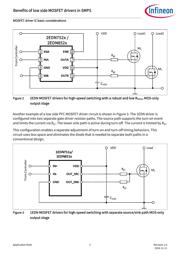
1.2.1 1EDN7511B/1EDN8511B separated outputs for source and sink.....................................................6
1.2.2 Reverse current capability – built-in diodes in the output stage avoid using external diodes.......7
1.2.3 Power dissipation in the driver..........................................................................................................8
1.2.4 MOSFET drive current capability.....................................................................................................10
1.2.5 Under voltage capability – reliable MOSFET protection.................................................................11
1.3 Propagation delay.................................................................................................................................12
1.4 Packaging ..............................................................................................................................................13
2 PCB design considerations...............................................................................................................15
2.1 Layout recommendations.....................................................................................................................15
2.2 Typical 2EDN layout snapshots ............................................................................................................16
2.3 Thermal recommendations ..................................................................................................................17
3 MOSFET driver tests .........................................................................................................................18
3.1 Testing robustness and testing different driver output stages ...........................................................18
3.2 Output reverse current test and comparison with other MOSFET drivers.......................................... 19
3.3 Output reverse current protection test with diodes............................................................................21
4 Conclusion .......................................................................................................................................23
5 References and proposed links ........................................................................................................24
6 Revision history................................................................................................................................25
Verzeichnis