

herunterladen

© 1999 Fairchild Semiconductor Corporation DS010945 www.fairchildsemi.com
September 1991
Revised November 1999
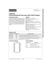
74ABT245 Octal Bi-Directional Transceiver with 3-STATE Outputs
74ABT245
Octal Bi-Directional Transceiver with 3-STATE Outputs
General Description
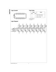
The ABT245 contains eight non-inverting bidirectional buff-
ers with 3-STATE outputs and is intended for bus-oriented
applications. Current sinking capability is 64 mA on both
the A and B ports. The Transmit/Receive (T/R
) input deter-
mines the direction of data flow through the bidirectional
transceiver. Transmit (active HIGH) enables data from A
Ports to B Ports; Receive (active LOW) enables data from
B Ports to A Ports. The Output Enable input, when HIGH,
disables both A and B ports by placing them in a HIGH Z
condition.
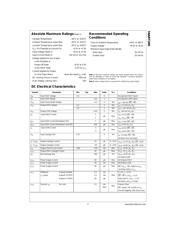
Features
■ Bidirectional non-inverting buffers
■ A and B output sink capability of 64 mA, source
capability of 32 mA
■ Guaranteed output skew
■ Guaranteed multiple output switching specifications
■ Output switching specified for both 50 pF and 250 pF
loads
■ Guaranteed simultaneous switching, noise level and
dynamic threshold performance
■ Guaranteed latchup protection
■ High impedance glitch-free bus loading during entire
power up and power down cycle
■ Non-destructive hot insertion capability
■ Disable time is less than enable time to avoid bus
contention
Ordering Code:
Device also available in Tape and Reel. Specify by appending suffix letter “X” to the ordering code.
Connection Diagram Pin Descriptions
Order Number Package Number Package Description
74ABT245CSC M20B 20-Lead Small Outline Integrated Circuit (SOIC), JEDEC MS-013, 0.300” Wide Body
74ABT245CSJ M20D 20-Lead Small Outline Package (SOP), EIAJ TYPE II, 5.3mm Wide
74ABT245CMSA MSA20 20-Lead Shrink Small Outline Package (SSOP), EIAJ TYPE II, 5.3mm Wide
74ABT245CMTC MTC20 20-Lead Thin Shrink Small Outline Package (TSSOP), JEDEC MO-153, 4.4mm Wide
74ABT245CPC N20A 20-Lead Plastic Dual-In-Line Package (PDIP), JEDEC MS-001, 0.300” Wide
Pin Names Description
OE
Output Enable Input (Active LOW)
T/R
Transmit/Receive Input
A
0
–A
7
Side A Inputs or 3-STATE Outputs
B
0
–B
7
Side B Inputs or 3-STATE Outputs
Verzeichnis
- ・ Konfiguration des Pinbelegungsdiagramms on Seite 1
- ・ Abmessungen des Paketumrisses on Seite 7 Seite 8 Seite 9 Seite 10 Seite 11
- ・ Teilenummerierungssystem on Seite 1
- ・ Typisches Anwendungsschaltbild on Seite 2
- ・ Beschreibung der Funktionen on Seite 1
- ・ Technische Daten on Seite 3
- ・ Elektrische Spezifikation on Seite 3 Seite 4