

herunterladen
AN-0972
APPLICATION NOTE
One Technology Way • P. O. Box 9106 • Norwood, MA 02062-9106, U.S.A. • Te l: 781.329.4700 • Fax: 781.461.3113 • www.analog.com
How the AD7329 Helps Reduce Costs
by Claire Croke and Jakub Szymczak
INTRODUCTION
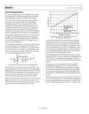
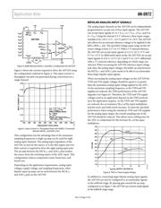
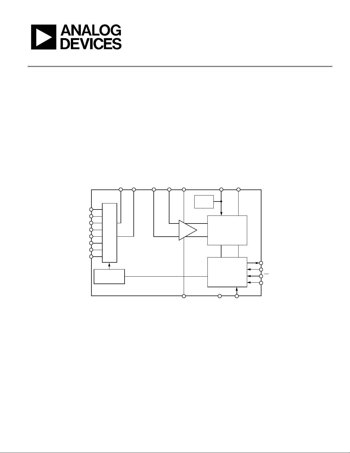
The AD7329 is an 8-channel, 12-bit plus one additional sign
bit, bipolar input ADC. The part has four software selectable
input ranges: ±4 × V
REF
, ±2 × V
REF
, ±V
REF
, and 0 to 4 × V
REF
. Each
analog input channel can be independently programmed to
one of the four analog input ranges. The AD7329 is manufactured
using the industrial CMOS (iCMOS®) process, which allows the
ADC to accept large bipolar analog input signals while providing
increased performance, reduced power consumption, and
reduced package size compared with other bipolar ADC solu-
tions available today.
The AD7329 boasts a very flexible design, which allows the
ADC to be configured to suit a wide variety of application
requirements. This application note outlines how to achieve
a very high input impedance from the AD7329 while retaining
the ability to accept large bipolar analog input signals. It also
discusses how the AD7329 can be configured to accommodate
small input signals while still maintaining high levels of
performance.
V
IN
0
V
IN
1
V
IN
2
V
IN
3
V
IN
4
V
IN
5
V
IN
6
V
IN
7
AD7329
AGNDV
SS
V
DRIVE
DIN
CS
SCLK
DOUT
V
CC
REF
IN
/
REF
OUT
V
DD
A
DC
IN
–
A
DC
IN
+MUX
OUT
+MUX
OUT
–
T/H
CHANNEL
SEQUENCER
13-BIT SUCCESSIVE
APPROXIMATION
ADC
CONTROL
LOGIC AND
REGISTERS
I/P
MUX
2.5V
VREF
07592-001
Figure 1. AD7329 Functional Block Diagram
Rev. 0 | Page 1 of 4