
herunterladen

AN-932
APPLICATION NOTE
One Technology Way • P. O. Box 9106 • Norwood, MA 02062-9106, U.S.A. • Te l: 781.329.4700 • Fax: 781.461.3113 • www.analog.com
Power Supply Sequencing
by Martin Murnane and Chris Augusta
Rev. 0 | Page 1 of 4
POWER-UP CONSIDERATIONS
Powering up a circuit on a printed circuit board is too often
taken for granted and can cause damage and both destructive
and nondestructive latch-up conditions. These problems may
not be prominent until volume production begins when the
tolerances of devices and designs are put to the test. This is
dangerously late in the process and extremely expensive, with
respect to time and the delivery of projects and products. Errors
found at this stage result in numerous modifications, including
PCB layout changes, design alterations, and extra anomalies.
With the advent of incorporating many functional blocks into
one integrated circuit (IC), this has resulted in supplying these
blocks with multiple, sometimes equal, or in many instances,
differing voltage supplies. As more and more of these system-
on-a-chip (SoC) ICs proliferate the marketplace, the need for
particular power supply sequencing and power management
issues arises.
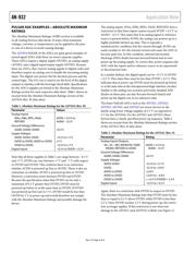
There is usually enough information in data sheets from Analog
Devices, Inc., to guide a designer to a correct power-up sequence
for an individual IC. However, some ICs specifically require a
well-defined power-up sequence. This is true in the case of
many of ICs from Analog Devices and is quite common in ones
using multiple supplies such as converters (consisting of both
analog-to-digital converters (ADCs) and digital-to-analog
converters (DACs)), digital signal processors (DSPs), audio/
video, radio frequency, and many other mixed signal ICs.
Essentially, any IC containing some analog input/output
with a digital engine falls into this category, where particular
power sequencing may be required. On these ICs, there could
be separate analog and digital supplies and some may even have
a digital input/output supply, as detailed in specific examples
discussed in the following sections.
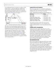
This application note looks at some of the more subtle power
supply issues that a designer must consider in new designs,
especially when there are several different power supplies
required for an IC. Some of the more common supplies
p r e s e n t l y a r e : + 1 . 8 V, + 2 . 0 V, + 2 . 5 V, + 3 . 3 V, + 5 V, − 5 V,
+12 V, and −12 V.
With over 10,000 different products worldwide from Analog
Devices, the scope of this application note looks only at a few
ADCs. However, these supply sequencing considerations can be
applied to practically any mixed signal IC from Analog Devices.