


herunterladen

AN-742
APPLICATION NOTE
One Technology Way • P. O. Box 9106 • Norwood, MA 02062-9106, U.S.A. • Te l: 781.329.4700 • Fax: 781.461.3113 • www.analog.com
Frequency Domain Response of Switched-Capacitor ADCs
by Rob Reeder
INTRODUCTION
Knowing the frequency response of unbuffered analog-to-
digital converters (ADCs) with a switched-capacitor front
end is an important first step in understanding how to design
an interface to these types of pipeline ADCs. The characteristic
input impedance that the ADC exhibits must be determined
before designing any high frequency interface, regardless of
whether it is active, passive, dc-coupled, or ac-coupled.
This application note develops a method, using measurements
made with a network analyzer, to provide a better under-
standing of the input response over high frequency ranges.
This allows users to design a more effective interface to
unbuffered converters with switched-capacitor inputs. All
measurements and model calculations were made using the
AD9236 in a 32-lead chip scale package (CSP).
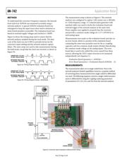
The converter’s internal sample-and-hold amplifier circuit
(SHA) is mainly comprised of an input switch, an input
sampling capacitor, a sampling switch, and an amplifier. As
Figure 1 shows, the input switch interfaces the driver circuit
with the input capacitor. When the input switch is on (track
mode), the driver circuit drives the input capacitor. The input
is sampled (captured) on the input capacitor at the end of this
mode. When the input switch is off (hold mode), the driver is
isolated from the input capacitor. The track mode period and
the hold mode period of the converter are approximately equal.
The interface problem with an unbuffered (switched-capacitor)
converter is seen as two fold—the frequency domain response,
which this application note presents, and time domain response.
The first issue is that the input impedance during the track
mode of the SHA is different from the input impedance during
the hold mode of the SHA. This makes it difficult to accurately
impedance match the converter’s input with the front-end
circuit for high IF designs. Since the converter samples at the
input signal only during the track mode, the input impedance
should be matched for this mode. The frequency dependence
of the input impedance is governed mainly by the sampling
capacitor and any parasitic capacitance in the signal path. For
accurate impedance matching, it is helpful to have an idea of the
frequency dependence of the input impedance. The measure-
ment results obtained from the AD9236 explain the behavior
of the input impedance over a wide range of input frequencies.
The Example section of this application note then shows a way
to determine an input interface with the converter during the
track mode.
The second problem lies in the time domain where the internal
switched-capacitor front end presents “kickback” into the driver
circuit. This problem occurs when the converter switches from
one mode to the other, charging the input capacitors from the
previous sample to the current sample. Therefore, the current
glitch occurring at the input of the converter is dependent on
three factors—the difference between the previous and the
current samples, the value of the input sampling capacitor, and
the sum of all resistances in the signal path (this is comprised
of the on resistance of the switches in the signal path and any
series resistance in the signal path).
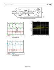
A time domain example of a current glitch seen at the analog
input pin is shown in Figure 2 and Figure 3. Figure 4 shows the
frequency domain content of the current glitch of the entire
network, in this case, on the primary side of a transformer-
coupled network.
If the nonlinear portion of the current glitch corrupts the input
sample when the driver has a linear response, the resulting
sampled signal will distort. Therefore, it is crucial to design
an input network (that is, a transformer or amplifier driver)
capable of settling the current glitch within a half-clock cycle
to preserve the converter’s performance.
Rev. B | Page 1 of 8