

herunterladen
AN-663
APPLICATION NOTE
One Technology Way • P.O. Box 9106 • Norwood, MA 02062-9106 • Tel: 781/329-4700 • Fax: 781/326-8703 • www.analog.com
This application note concentrates on the AD7739 but is
also applicable to the AD7732, AD7734, and AD7738.The
purpose of this application note is to explore the calibration
registers in more detail than is found on the data sheets.
INTRODUCTION
The AD7739 features two sets of calibration registers. The
main function of these registers is to store the offset and gain
coefcients for the various calibration modes. However,
since all nine sets of registers can be read to and written
from over the serial interface, these registers are available
to manipulate raw ADC conversion results.
The rst set of registers is a 24-bit offset (ADC offset)
register and 24-bit gain (ADC gain) register, which affect
all channels. The second set includes a per channel 24-bit
offset register and a 24-bit per channel gain register, which
affect a specic channel only.
AD7732/AD7734/AD7738/AD7739 Calibration Registers
By Tom Meany
The effect of the calibration registers is independent of
conversion time, but does depend on the range. All calibra-
tion registers on the AD7732, AD7734, AD7738, and AD7739
can be read to or written from over the serial interface.
However, a write to the registers will be ignored if the ADC
is converting or calibrating when the write takes place.
This avoids corrupting the conversion result. Therefore,
you must set the ADC into its sync mode by writing 000
to the mode bits before writing to any of the calibration
registers.
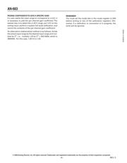
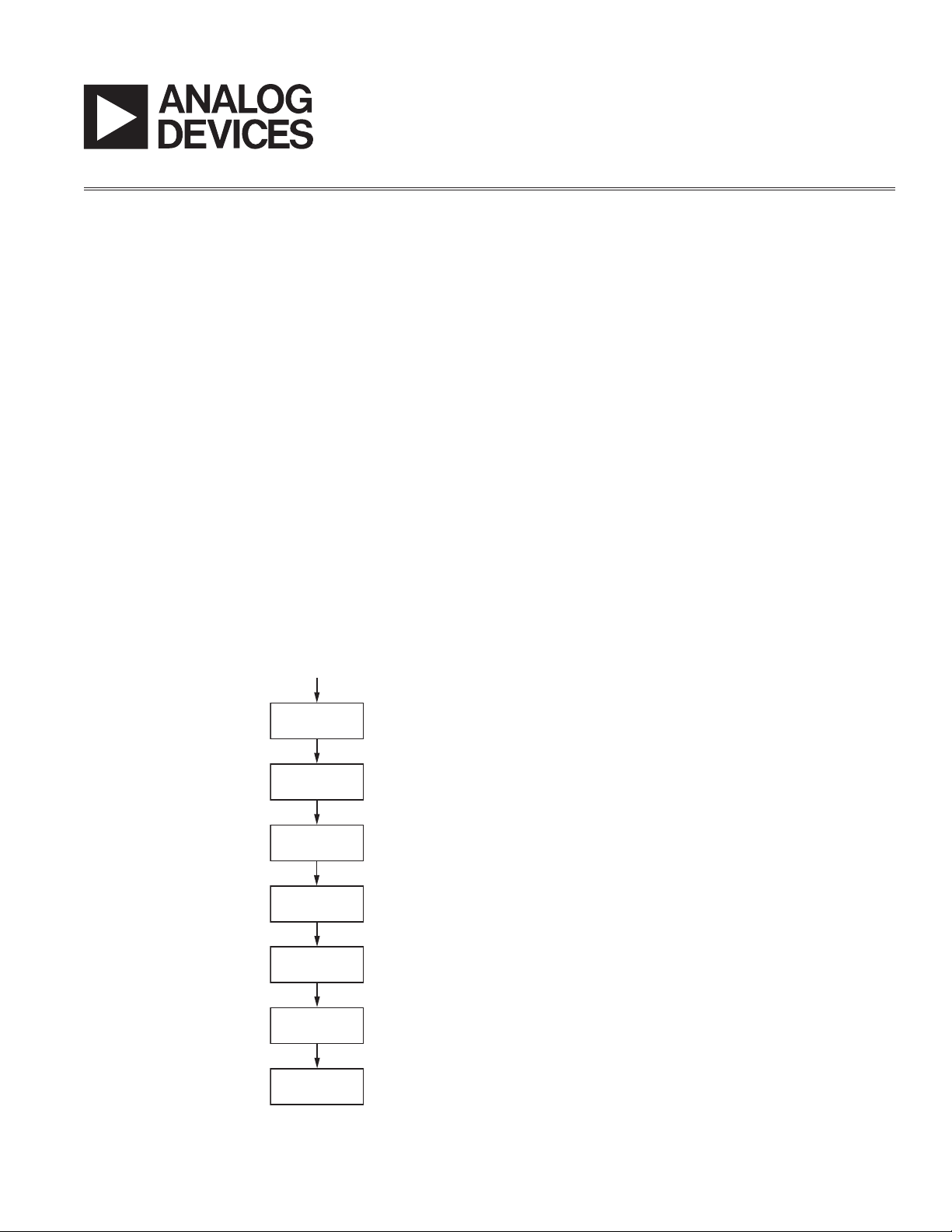
FOR UNIPOLAR RANGES:
DATA = ((ADC RESULT – R ADC ZS CAL. REG.) XADC FS REG./
200000h – R CH. ZS CAL. REG.) XCH. FS CAL. REG./200000h
FOR BIPOLAR RANGES:
DATA = ((ADC RESULT – R ADC ZS CAL. REG.) XADC FS REG./
400000h + 800000h – R CH. ZS CAL. REG.) XCH. FS CAL. REG./200000h
WHERE THE ADC RESULT IS IN THE RANGE OF 0 TO FFFFFh.
AND R = 1 ON 2.5 V AND 1.25 V RANGES AND R = 2 ON THE 0.625 V.
CONVERSION
DATA
AVAILABLE
SUBTRACT
ADC OFFSET
REGISTER
MULTIPLY BY
ADC GAIN
REGISTER
SUBTRACT
PER CHANNEL
OFFSET REGISTER
MULTIPLY BY
PER CHANNEL
GAIN REGISTER
APPLY CLAMP
IF SELECTED
WRITE TO
DATA REGISTER
FROM FILTER
Figure 1. Flow Chart for Calibration Register Contents
REV. 0