


herunterladen
50 MHz to 3.5 GHz, 45 dB
RF Detector
AD8312
Rev. 0
Information furnished by Analog Devices is believed to be accurate and reliable.
However, no responsibility is assumed by Analog Devices for its use, nor for any
infringements of patents or other rights of third parties that may result from its use.
Specifications subject to change without notice. No license is granted by implication
or otherwise under any patent or patent rights of Analog Devices. Trademarks and
registered trademarks are the property of their respective owners.
One Technology Way, P.O. Box 9106, Norwood, MA 02062-9106, U.S.A.
Tel: 781.329.4700
www.analog.com
Fax: 781.461.3113 © 2005 Analog Devices, Inc. All rights reserved.
FEATURES
Complete RF detector function
Typical range: −45 dBm to 0 dBm, re 50 Ω
Frequency response from 50 MHz to 3.5 GHz
Temperature-stable linear-in-dB response
Accurate to 3.5 GHz
Rapid response: 85/120 ns (rise/fall)
Low power: 12 mW at 2.7 V
APPLICATIONS
Cellular handsets (GSM, CDMA, WCDMA)
RSSI and TSSI for wireless terminal devices
Transmitter power measurement
GENERAL DESCRIPTION
The AD8312 is a complete, low cost subsystem for the
measurement of RF signals in the frequency range of 50 MHz to
3.5 GHz. It has a typical dynamic range of 45 dB and is intended
for use in a wide variety of cellular handsets and other wireless
devices. It provides a wider dynamic range and better accuracy
than possible using discrete diode detectors. In particular, its
temperature stability is excellent over the full operating range of
−40°C to +85°C.
Its high sensitivity allows measurement at low power levels, thus
reducing the amount of power that needs to be coupled to the
detector. It is essentially a voltage-responding device, with a
typical signal range of 1.25 mV to 224 mV rms or −45 dBm to
0 dBm, re 50 Ω.
For convenience, the signal is internally ac-coupled, using a
5 pF capacitor to a load of 3 kΩ in shunt with 1.3 pF. This high-
pass coupling, with a corner at approximately 16 MHz,
determines the lowest operating frequency. Therefore, the
source may be dc grounded.
The AD8312 output, VOUT, increases from close to ground to
about 1.2 V because the input signal level increases from
1.25 mV to 224 mV. A capacitor may be connected between the
VOUT and CFLT pins when it is desirable to increase the time
interval over which averaging of the input waveform occurs.
The AD8312 is available in a 6-ball, 1.0 mm × 1.5 mm, wafer-
level chip scale package and consumes 4.2 mA from a 2.7 V to
5.5 V supply.
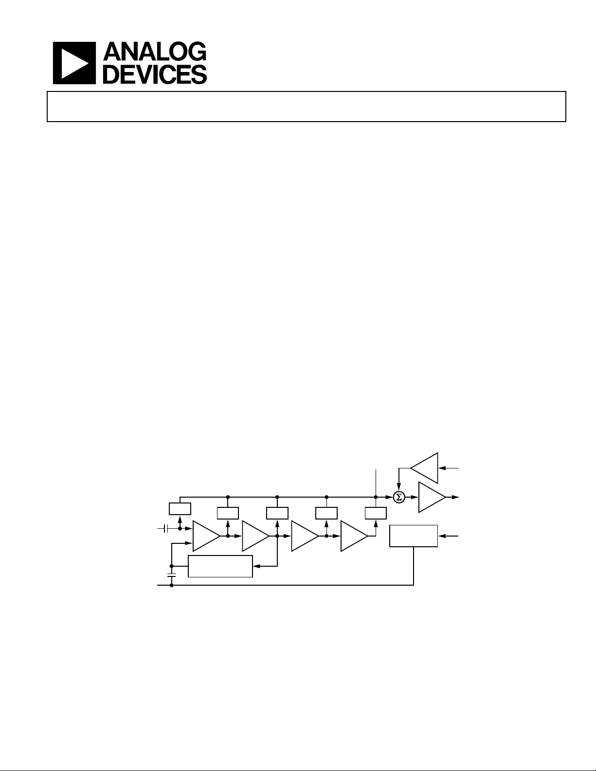
FUNCTIONAL BLOCK DIAGRAM
05260-001
10dB
DET
10dB
DET
10dB
DET
10dB
DET
DET
+
–
CFLT
RFIN
COMM
OFFSET
COMPENSATION
V-I
VSET
BAND-GAP
REFERENCE
VPOS
I-V
VOUT
AD8312
Figure 1.