
herunterladen
AN-1142
APPLICATION NOTE
One Technology Way • P. O. Box 9106 • Norwood, MA 02062-9106, U.S.A. • Tel: 781.329.4700 • Fax: 781.461.3113 • www.analog.com
Techniques for High Speed ADC PCB Layout
by Rob Reeder
Rev. 0 | Page 1 of 8
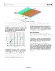
INTRODUCTION
In today’s industry, the layout of the system board has become
an integral part of the design itself. Therefore, it is of paramount
importance that the designer has an understanding of the
mechanisms that affect the performance of a high speed signal
chain design.
There are many options to consider when it comes to laying
out a printed circuit board (PCB) in a high speed analog signal
chain design. Some options matter more than others, and some
are application dependent. In the end, the answer varies but in
all cases the designer should try to lean on the error of best
practice without becoming overly critical regarding every layout
detail. This application note provides information that may be
useful when starting the next high speed design.
EXPOSED PADDLES
Exposed paddles, or EPADs, are sometimes overlooked; how-
ever, they are essential to getting the most performance out
of the signal chain as well as getting the most heat out of
the device.
The exposed paddle, referred to at Analog Devices, Inc., as
Pin 0, is the paddle found underneath most parts today. This
is an important connection because it ties all internal grounds
from the die to a central point under the part. Note the lack of
ground pins in many converters and amplifiers today. The
EPAD is the reason why.
The key is to tie this pin down, that is, soldered well to the PCB
to make a robust electrical and thermal connection. When this
connection is not solid, havoc can occur. In other words, the
design may not work.
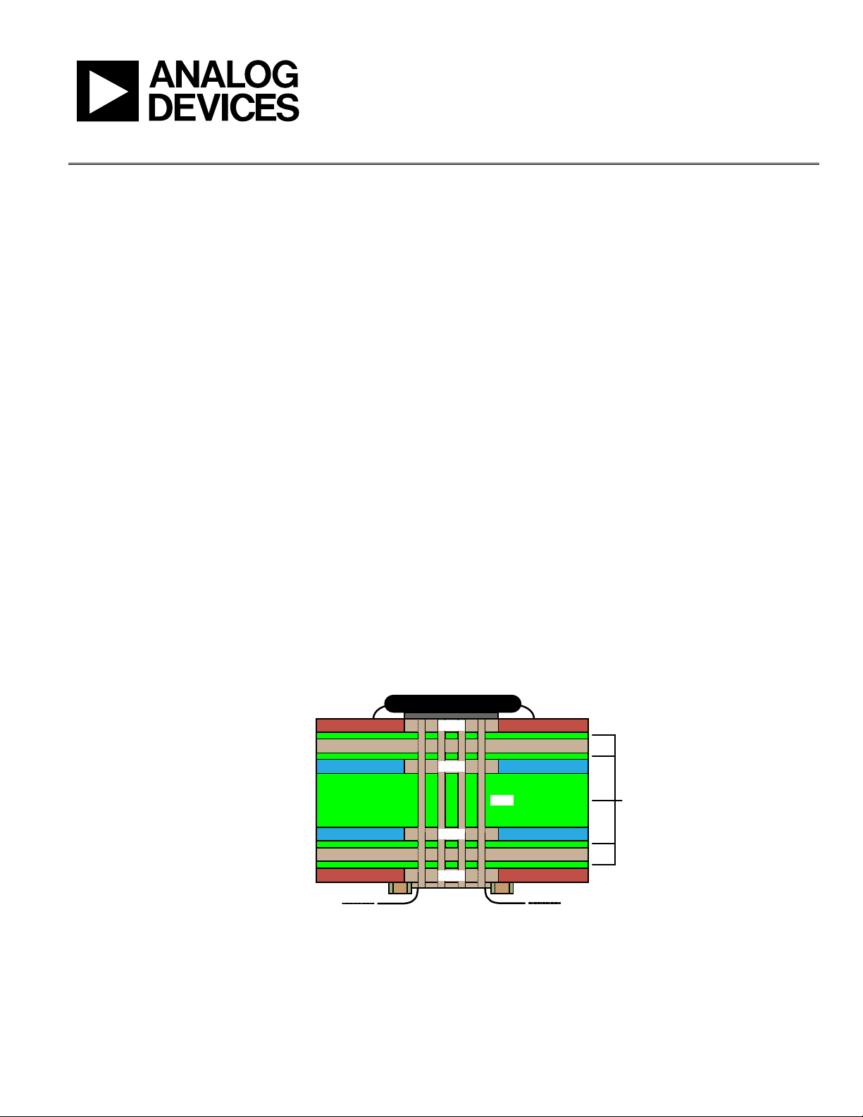
Achieving the Best Connection
There are three basic steps to take to achieve the best con-
nection, electrically and thermally, with the EPAD. First, if
possible, replicate the EPA D on each PCB layer. Doing so
creates a thick thermal connection to all grounds and ground
layers so that the heat can dissipate and spread out quickly. This
is pertinent for high power parts and for applications that have
high channel counts. Electrically, this gives a good equal con-
nection to all the ground layers.
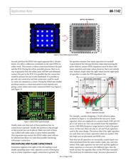
One can even replicate the EPA D on the bottom layer (see
Figure 1). This can serve as a thermal relief ground point for
decoupling and a placeholder to attach a heat sink on the
bottom side.
ADC
DECOUPLING CAP
10484-001
DECOUPLING CAP
LAYER 1 - TOP SIGNAL
LAYER 2 - GROUND1
LAYER 3 - POWER1
LAYER 5 - GROUND2
LAYER 6 - BOTTOM SIGNAL
LAYER 4 - POWER2
DIELECTRIC
LAYERS
EPAD
EPAD
EPAD
EPAD
VIAS
Figure 1. Exposed Pad Layer Layout Example