


herunterladen
5
6
3
4
1
©
1996 Burr-Brown Corporation AB-106A Printed in U.S.A. August, 1997
PROGRAMMING TRICKS FOR HIGHER CONVERSION
SPEEDS UTILIZING DELTA SIGMA CONVERTERS
By Bonnie Baker
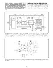
balancing A/D converter, a calibration µC with on-chip static
RAM, a clock oscillator, a programmable digital filter, and a bi-
directional serial communications port. The function of the
multi-order charge-balancing A/D converter can be conceptual-
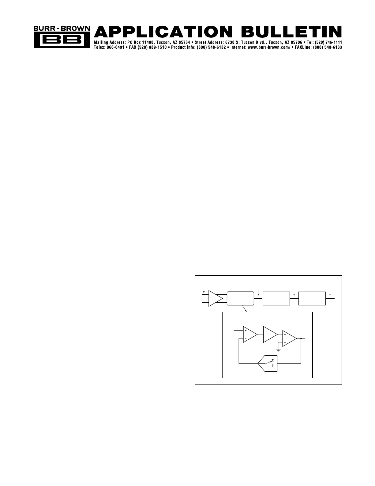
ized with the first-order stage shown in the insert in Figure 1.
The analog input voltage and the output of the 1-bit DAC is
differentiated, providing an analog voltage at X
2
. The voltage at
X
2
is presented to the integrator. The output of the integrator
progresses in a negative or positive direction. The slope and
direction of the signal at X
3
is dependant on the sign and
magnitude of X
2
. At the time the voltage at X
3
equals the
comparator reference voltage, the output of the comparator
switches from negative to positive or positive to negative,
dependent on its original state. The output value of the com-
parator (X
4
) is clocked into the 1-bit DAC, as well as clocked
into the digital filter stage. At the time that the output of the
comparator switches from a HIGH to a LOW or visa versa, the
1-bit DAC responds on the next clock pulse by changing its
analog output voltage to the difference amplifier. This creates
a different output voltage at X
2
, causing the integrator to
progress in the opposite direction.
Delta-Sigma (∆Σ) Analog-to-Digital Converters are well known
for their innate ability to resolve an analog input signal to very
small LSB voltage ranges. The primarily applications for this
type of product is in the Industrial Process Control market such
as direct transducer interface for pressure, temperature, flow,
weigh scales and force measurement systems. In the Instrumen-
tation market, the ∆Σ converter is particularly well-suited for
portable applications, such as thermometers, gas analyzers and
blood analyzers. At first glance, high resolution doesn’t seem to
be an important specification for these types of applications. To
the contrary, close inspection of these transducer interface
circuits divulge a different story. The sensing element’s output
could be a fairly high voltage (hundreds of mV to several volts),
however, the delta output voltages that represent a change in
temperature, pressure, light, etc., is usually extremely low, sub-
mV or µV. If the dynamic resolution of the A/D converter is
relatively high, the total application cost can be lowered. Addi-
tionally, the circuit becomes less complex making it easier to
design. ∆Σ ADCs are very good in the right application but they
do have some disadvantages. The most obvious of these is a
limited frequency response. The frequency response is dictated
by the output data rate. A greater data rate leads to a higher
frequency response but lower effective resolution. Although the
∆Σ converter brings the circuit designer considerably closer to
achieving the desired results, expanding the application to
include µP implemented bit-shifting or front end analog gain
techniques can enhance the resolution even further (refer to
AB-107 for more details about front end analog gain). The
technique of shifting the output bits of the A/D converter in the
µP is not new, however, a revisit is appropriate in lieu of the
arrival of the ∆Σ converter, where higher resolution is possible
in the conversion process. This Application Bulletin addresses
the design trade-off that is taken between resolution and data
rates when ∆Σ converters are used. This relationship is exam-
ined and techniques such as hardware and software gain are
used. These techniques can be used as tools to improve the
resolution versus data rate picture. In this Application Bulletin
the advantages of software gain emphasized.
The fundamental concept of the original ∆Σ A/D conversion
process was based on a single-bit quantizer, rather than multi-
bit, as used in architectures such as sub-ranging or successive
approximation. Since the first design of the ∆Σ A/D converters
front ends have been designed that digitize more than 1-bit of
resolution, while tolerating some design trade-offs for the
multi-bit approach. The state-of-the-art ∆Σ converter contains a
programmable gain amplifier (PGA), a multi-order charge-
FIGURE 1. A Block Diagram of a Generic
∆Σ
A/D Converter.
Typically, this class of modulator has an input Programmable Gain
Amplifier that conditions the analog input signal. The PGA stage is
followed by the multi-order charge-balancing section which per-
forms the first step in low frequency noise reduction and digitizes the
signal into a stream of ones and zeros. This stage is followed by a
digital low pass filter and finally, a decimation stage. The digital low-
pass filter and decimation filter can be combined in some A/D
converters, dependent on the design topology used.
PGA
Analog
Input
Multi-Order
Charge-Balancing
A/D Converter
Digital
Low-Pass
Filter
1st-Order Modulator
Integrator
∫
1-Bit DAC
Difference
Amp
X
2
X
5
X
3
X
4
Analog
Input
Comparator
(1-Bit ADC)
Decimation
Filter
1-Bit Data
Stream
Multi-Bit
Data
Multi-Bit
Output Data
®
SBAA005
Verzeichnis
- ・ Blockdiagramm on Seite 1
- ・ Technische Daten on Seite 4