

herunterladen
2010 Microchip Technology Inc. DS01311A-page 1
AN1311
INTRODUCTION
Currently, many portable battery-powered applications
use multiple cell batteries for power. In some cases, the
product form factor is driven by the size of the battery
pack.
This application note introduces and details design
equations and trade-offs that facilitate the use of single
cell input synchronous boost converters from the
Microchip MCP1640/B/C/D family of devices.
These single cell input boost converters enable startup
from very low input voltage sources. The
MCP1640/B/C/D converters will start from a 0.65 V
source and operate down to 0.35 V, while boosting the
output voltage from 2.0 V to 5.5 V. Two typical
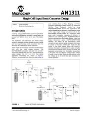
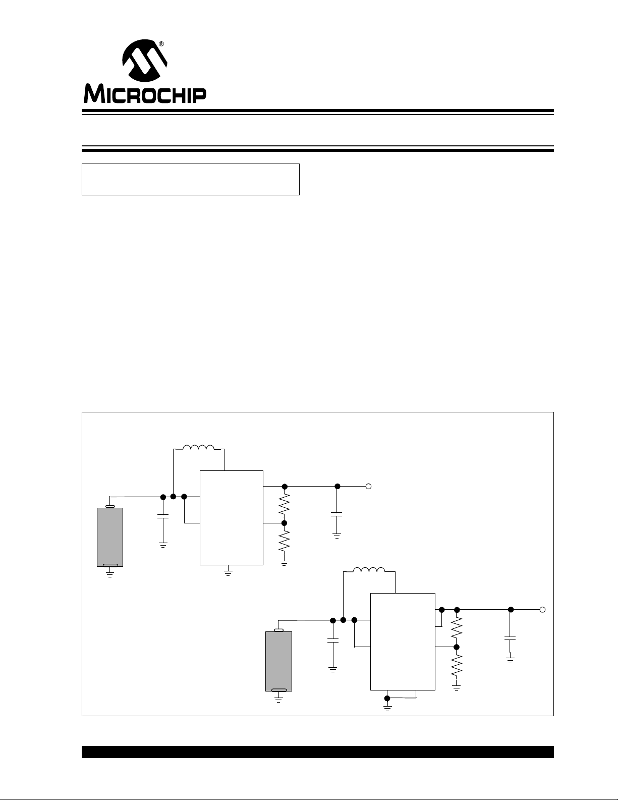
application schematics are shown in Figure 1.
Efficiency is maximized over the entire load range by
auto switching from a Pulse Skipping, or Pulse
Frequency Modulation (PFM) mode to a continuous
500 kHz Fixed Frequency mode by using
MCP1640/MCP1640C devices. For applications that
cannot tolerate the low frequency Pulse Skipping mode
or the output ripple voltage associated with it, the
MCP1640B/D devices switch at a continuous fixed
pulse width modulation frequency of 500 kHz. In
addition to dual switching modes, the MCP1640/B/C/D
family of devices offers two disable options. In the True
Output Disconnect option (MCP1640/MCP1640B
devices), the output of the synchronous boost
converter is open and the typical diode path from input
to output is removed, isolating the input from the
output. In the Input Bypass option (MCP1640C/D
devices), the input is connected to the output using the
synchronous P-Channel switch. During this mode, the
quiescent current draw from the battery is less than
1 µA typical. The Input Bypass mode provides voltage
to power a load in deep sleep with the ability to boost
the voltage up to the levels that are necessary for
normal operation.
FIGURE 1: Typical MCP1640 Applications.
Author: Terry Cleveland
Microchip Technology Inc.
V
IN
GND
V
FB
SW
V
IN
0.9 V to 1.7 V
V
OUT
3.3 V @ 100 mA
C
OUT
10 µF
C
IN
4.7 µF
L
1
4.7 µH
V
OUT
+
-
976 K
562 K
Alkaline
EN
V
IN
P
GND
V
FB
SW
V
IN
3.0 V to 4.2 V
V
OUT
5.0 V @ 200 mA
C
OUT
10 µF
C
IN
4.7 µF
L
1
4.7 µH
V
OUTS
+
-
976 K
309 K
V
OUTP
S
GND
Li-Ion
EN
Single Cell Input Boost Converter Design