
herunterladen
AFT18H357--24SR6
1
RF Device Data
Freescale Semiconductor, Inc.
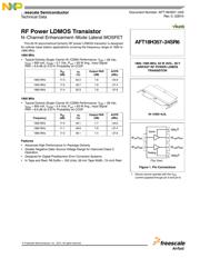
RF Power LDMOS Transistor
N--Channel Enhancement--Mode Lateral MOSFET
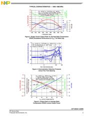
This 63 W asymmetrical Doherty RF power LDMOS trans istor is designed
for cellular base station applications c ov ering the frequency range of 1805 to
1995 MHz.
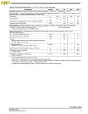
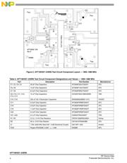
1800 MHz
Typical Doherty Single--Carrier W--CDMA Performance: V
DD
=28Vdc,
I
DQA
= 800 mA, V
GSB
=0.7Vdc,P
out
= 63 W Avg., Input Signal
PAR = 9.9 dB @ 0.01% Probability on CCDF.
G
ps
(dB)
D
(%)
Output PAR
(dB)
ACPR
(dBc)
1805 MHz 17.3 50.3 7.8 --34.6
1840 MHz 17.5 49.7 7.9 --37.4
1880 MHz 17.4 50.3 7.8 --37.6
1900 MHz
Typical Doherty Single--Carrier W--CDMA Performance: V
DD
=28Vdc,
I
DQA
= 800 mA, V
GSB
=0.4Vdc,P
out
= 63 W Avg., Input Signal
PAR = 9.9 dB @ 0.01% Probability on CCDF.
Frequency
G
ps
(dB)
D
(%)
Output PAR
(dB)
ACPR
(dBc)
1930 MHz 17.0 49.1 7.7 --34.6
1960 MHz 17.1 48.9 7.6 --37.4
1995 MHz 17.0 49.1 7.4 --37.6
Features
Advanced High Performance In--Package Doherty
Greater Negative Gate--Source Voltage Range for Improved Class C
Operation
Designed for Digital Predistortion Error Correction Systems
In Tape and Reel. R6 Suffix = 150 Units, 56 mm Tape Width, 13--inch Reel.
Document Number: AFT18H357--24S
Rev. 0, 3/2014
Freescale Semiconductor
Technical Data
1805–1995 MHz, 63 W AVG., 28 V
AIRFAST RF POWER LDMOS
TRANSISTOR
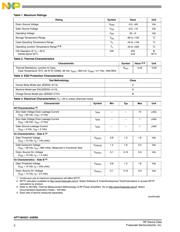
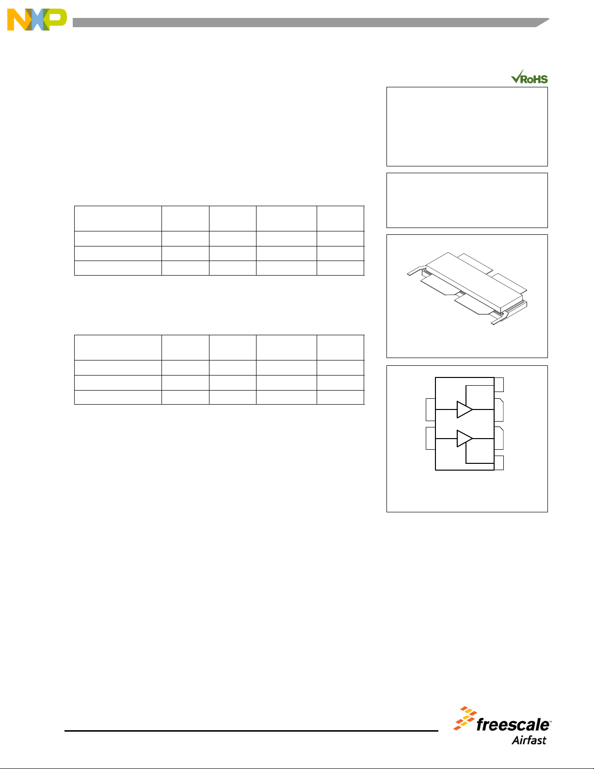
AFT18H357--24SR6
NI--1230S--4L2L
(Top View)
RF
outA
/V
DSA
RF
outB
/V
DSB
RF
inA
/V
GSA
RF
inB
/V
GSB
VBW
A
(1)
6
3
15
24
Carrier
Peaking
Figure 1. Pin Connections
VBW
B
(1)
1. Device cannot operate with the V
DD
current supplied through pin 3 and pin 6.
Freescale Semiconductor, Inc., 2014.
A
ll rights reserved.
Verzeichnis