
herunterladen
Semiconductor Components Industries, LLC, 2011
November, 2011 − Rev. 8
1 Publication Order Number:
BC856BDW1T1/D
BC856BDW1T1G,
SBC856BDW1T1GSeries,
BC857BDW1T1G,
SBC857BDW1T1GSeries,
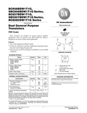
BC858CDW1T1G Series
Preferred Devices
Dual General Purpose
Transistors
PNP Duals
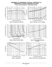
These transistors are designed for general purpose amplifier
applications. They are housed in the SOT−363/SC−88 which is
designed for low power surface mount applications.
Features
AEC−Q101 Qualified and PPAP Capable
S Prefix for Automotive and Other Applications Requiring Unique
Site and Control Change Requirements
These Devices are Pb−Free, Halogen Free/BFR Free and are RoHS
Compliant*
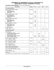
MAXIMUM RATINGS
Rating Symbol Value Unit
Collector−Emitter Voltage
BC856, SBC856
BC857, SBC857
BC858
V
CEO
−65
−45
−30
V
Collector−Base Voltage
BC856, SBC856
BC857, SBC857
BC858
V
CBO
−80
−50
−30
V
Emitter−Base Voltage V
EBO
−5.0 V
Collector Current −Continuous I
C
−100 mAdc
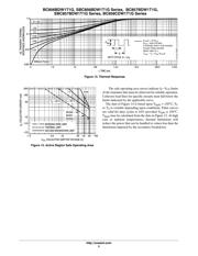
THERMAL CHARACTERISTICS
Characteristic Symbol Max Unit
Total Device Dissipation Per Device
FR−5 Board (Note 1)
T
A
= 25C
Derate Above 25C
P
D
380
250
3.0
mW
mW/C
mW/C
Thermal Resistance,
Junction−to−Ambient
R
q
JA
328
C/W
Junction and Storage Temperature
Range
T
J
, T
stg
−55 to +150 C
Stresses exceeding Maximum Ratings may damage the device. Maximum
Ratings are stress ratings only. Functional operation above the Recommended
Operating Conditions is not implied. Extended exposure to stresses above the
Recommended Operating Conditions may affect device reliability.
1. FR−5 = 1.0 x 0.75 x 0.062 in
*For additional information on our Pb−Free strategy and soldering details, please
download the ON Semiconductor Soldering and Mounting Techniques
Reference Manual, SOLDERRM/D.
SOT−363/SC−88
CASE 419B
STYLE 1
MARKING DIAGRAM
Preferred devices are recommended choices for future use
and best overall value.
Q
1
(1)(2)
(3)
(4) (5) (6)
Q
2
http://onsemi.com
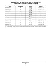
See detailed ordering and shipping information in the package
dimensions section on page 6 of this data sheet.
ORDERING INFORMATION
3x = Specific Device Code
x = B, F, G, or L
(See Ordering Information)
M = Date Code
G =Pb−Free Package
3x MG
G
1
6
(Note: Microdot may be in either location)
Verzeichnis