

herunterladen
© Semiconductor Components Industries, LLC, 2014
November, 2014 − Rev. 15
1 Publication Order Number:
BDX53B/D
BDX53B, BDX53C (NPN),
BDX54B, BDX54C (PNP)
Plastic Medium-Power
Complementary Silicon
Transistors
These devices are designed for general−purpose amplifier and
low−speed switching applications.
Features
• High DC Current Gain −
h
FE
= 2500 (Typ) @ I
C
= 4.0 Adc
• Collector Emitter Sustaining Voltage − @ 100 mAdc
V
CEO(sus)
= 80 Vdc (Min) − BDX53B, 54B
V
CEO(sus)
= 100 Vdc (Min) − BDX53C, 54C
• Low Collector−Emitter Saturation Voltage −
V
CE(sat)
= 2.0 Vdc (Max) @ I
C
= 3.0 Adc
V
CE(sat)
= 4.0 Vdc (Max) @ I
C
= 5.0 Adc
• Monolithic Construction with Built−In Base−Emitter Shunt Resistors
• These Devices are Pb−Free and are RoHS Compliant*
ÎÎÎÎÎÎÎÎÎÎÎÎÎÎÎÎÎÎÎ
ÎÎÎÎÎÎÎÎÎÎÎÎÎÎÎÎÎÎÎ
MAXIMUM RATINGS
ÎÎÎÎÎÎÎÎÎÎÎÎ
ÎÎÎÎÎÎÎÎÎÎÎÎ
Rating
ÎÎÎ
ÎÎÎ
Symbol
ÎÎÎÎ
ÎÎÎÎ
Value
ÎÎÎ
ÎÎÎ
Unit
ÎÎÎÎÎÎÎÎÎÎÎÎ
ÎÎÎÎÎÎÎÎÎÎÎÎ
ÎÎÎÎÎÎÎÎÎÎÎÎ
Collector−Emitter Voltage
BDX53B, BDX54B
BDX53C, BDX54C
ÎÎÎ
ÎÎÎ
ÎÎÎ
V
CEO
ÎÎÎÎ
ÎÎÎÎ
ÎÎÎÎ
80
100
ÎÎÎ
ÎÎÎ
ÎÎÎ
Vdc
ÎÎÎÎÎÎÎÎÎÎÎÎ
ÎÎÎÎÎÎÎÎÎÎÎÎ
ÎÎÎÎÎÎÎÎÎÎÎÎ
ÎÎÎÎÎÎÎÎÎÎÎÎ
Collector−Base Voltage
BDX53B, BDX54B
BDX53C, BDX54C
ÎÎÎ
ÎÎÎ
ÎÎÎ
ÎÎÎ
V
CB
ÎÎÎÎ
ÎÎÎÎ
ÎÎÎÎ
ÎÎÎÎ
80
100
ÎÎÎ
ÎÎÎ
ÎÎÎ
ÎÎÎ
Vdc
ÎÎÎÎÎÎÎÎÎÎÎÎ
Emitter−Base Voltage
ÎÎÎ
V
EB
ÎÎÎÎ
5.0
ÎÎÎ
Vdc
ÎÎÎÎÎÎÎÎÎÎÎÎ
ÎÎÎÎÎÎÎÎÎÎÎÎ
ÎÎÎÎÎÎÎÎÎÎÎÎ
Collector Current − Continuous
− Peak
ÎÎÎ
ÎÎÎ
ÎÎÎ
I
C
ÎÎÎÎ
ÎÎÎÎ
ÎÎÎÎ
8.0
12
ÎÎÎ
ÎÎÎ
ÎÎÎ
Adc
ÎÎÎÎÎÎÎÎÎÎÎÎ
ÎÎÎÎÎÎÎÎÎÎÎÎ
Base Current
ÎÎÎ
ÎÎÎ
I
B
ÎÎÎÎ
ÎÎÎÎ
0.2
ÎÎÎ
ÎÎÎ
Adc
ÎÎÎÎÎÎÎÎÎÎÎÎ
ÎÎÎÎÎÎÎÎÎÎÎÎ
Total Device Dissipation @ T
C
= 25°C
Derate above 25°C
ÎÎÎ
ÎÎÎ
P
D
ÎÎÎÎ
ÎÎÎÎ
65
0.48
ÎÎÎ
ÎÎÎ
W
W/°C
ÎÎÎÎÎÎÎÎÎÎÎÎ
ÎÎÎÎÎÎÎÎÎÎÎÎ
ÎÎÎÎÎÎÎÎÎÎÎÎ
Operating and Storage Junction
Temperature Range
ÎÎÎ
ÎÎÎ
ÎÎÎ
T
J
, T
stg
ÎÎÎÎ
ÎÎÎÎ
ÎÎÎÎ
−65 to +150
ÎÎÎ
ÎÎÎ
ÎÎÎ
°C
Stresses exceeding those listed in the Maximum Ratings table may damage the
device. If any of these limits are exceeded, device functionality should not be
assumed, damage may occur and reliability may be affected.
ÎÎÎÎÎÎÎÎÎÎÎÎÎÎÎÎÎÎÎ
ÎÎÎÎÎÎÎÎÎÎÎÎÎÎÎÎÎÎÎ
THERMAL CHARACTERISTICS
ÎÎÎÎÎÎÎÎÎÎÎÎ
ÎÎÎÎÎÎÎÎÎÎÎÎ
Characteristic
ÎÎÎ
ÎÎÎ
Symbol
ÎÎÎÎ
ÎÎÎÎ
Max
ÎÎÎ
ÎÎÎ
Unit
ÎÎÎÎÎÎÎÎÎÎÎÎ
Thermal Resistance, Junction−to−Ambient
ÎÎÎ
R
q
JA
ÎÎÎÎ
70
ÎÎÎ
°C/W
ÎÎÎÎÎÎÎÎÎÎÎÎ
ÎÎÎÎÎÎÎÎÎÎÎÎ
Thermal Resistance, Junction−to−Case
ÎÎÎ
ÎÎÎ
R
q
JC
ÎÎÎÎ
ÎÎÎÎ
1.92
ÎÎÎ
ÎÎÎ
°C/W
*For additional information on our Pb−Free strategy and soldering details, please
download the ON Semiconductor Soldering and Mounting Techniques
Reference Manual, SOLDERRM/D.
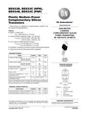
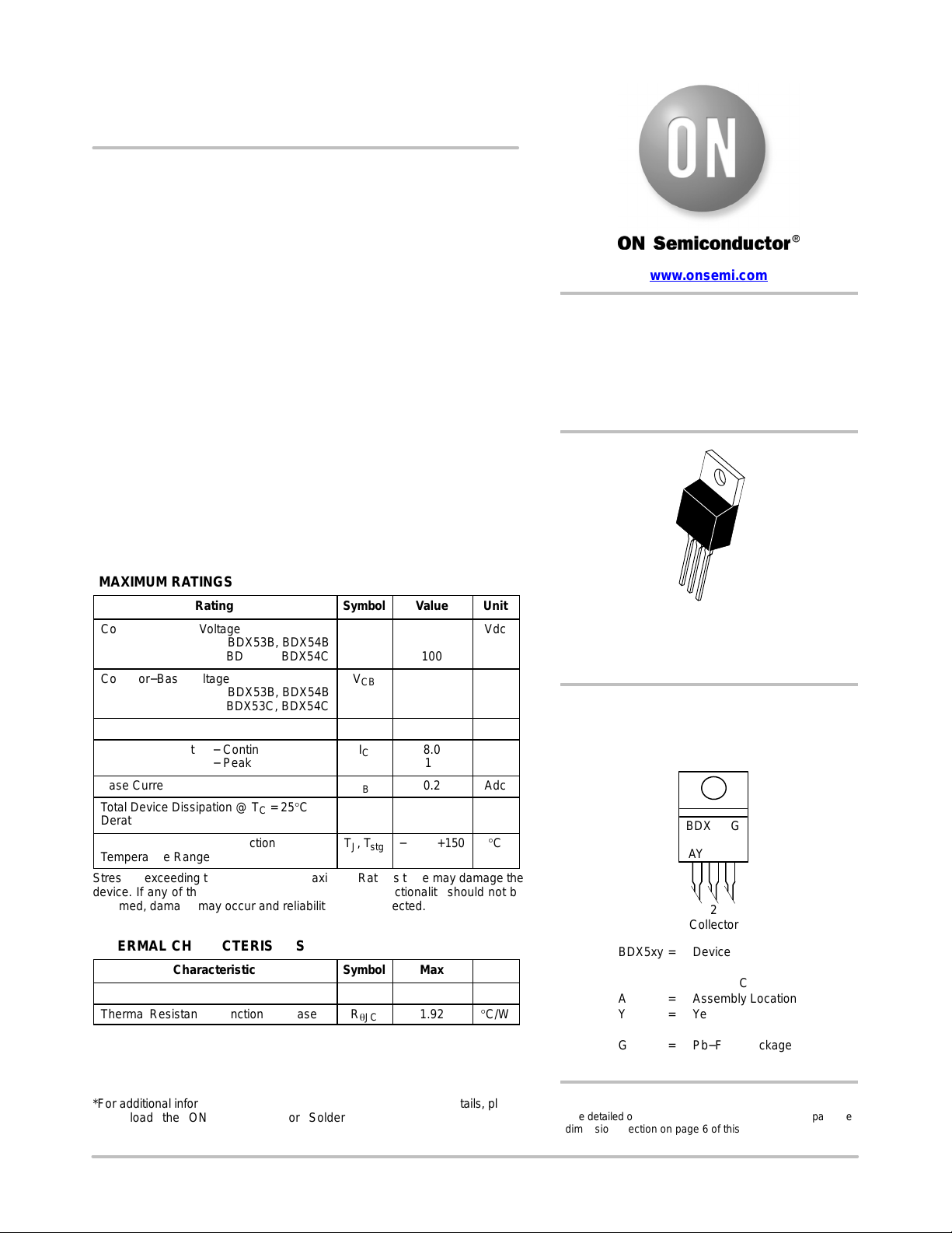
DARLINGTON
8 AMPERE
COMPLEMENTARY SILICON
POWER TRANSISTORS
80−100 VOLTS, 65 WATTS
TO−220
CASE 221A
STYLE 1
1
2
3
4
MARKING DIAGRAM
& PIN ASSIGNMENT
1
Base
3
Emitter
4
Collector
2
Collector
www.onsemi.com
BDX5xy = Device Code
x = 3 or 4
y = B or C
A = Assembly Location
Y = Year
WW = Work Week
G = Pb−Free Package
BDX5xyG
AY WW
See detailed ordering and shipping information in the package
dimensions section on page 6 of this data sheet.
ORDERING INFORMATION
Verzeichnis
- ・ Konfiguration des Pinbelegungsdiagramms on Seite 1
- ・ Abmessungen des Paketumrisses on Seite 7
- ・ Teilenummerierungssystem on Seite 1 Seite 6 Seite 7
- ・ Markierungsinformationen on Seite 1 Seite 7
- ・ Blockdiagramm on Seite 6
- ・ Technische Daten on Seite 6
- ・ Elektrische Spezifikation on Seite 2
- ・ Teilenummernliste on Seite 1