
herunterladen
© Semiconductor Components Industries, LLC, 2014
November, 2014 − Rev. 8
1 Publication Order Number:
BUL45D2/D
BUL45D2G
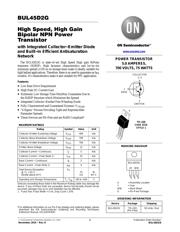
High Speed, High Gain
Bipolar NPN Power
Transistor
with Integrated Collector−Emitter Diode
and Built−in Efficient Antisaturation
Network
The BUL45D2G is state−of−art High Speed High gain BiPolar
transistor (H2BIP). High dynamic characteristics and lot−to−lot
minimum spread (±150 ns on storage time) make it ideally suitable for
light ballast applications. Therefore, there is no need to guarantee an h
FE
window. It’s characteristics make it also suitable for PFC application.
Features
• Low Base Drive Requirement
• High Peak DC Current Gain
• Extremely Low Storage Time Min/Max Guarantees Due to
the H2BIP Structure which Minimizes the Spread
• Integrated Collector−Emitter Free Wheeling Diode
• Fully Characterized and Guaranteed Dynamic V
CE(sat)
• “6 Sigma” Process Providing Tight and Reproductible
Parameter Spreads
• These Devices are Pb−Free and are RoHS Compliant*
MAXIMUM RATINGS
Rating Symbol Value Unit
Collector−Emitter Sustaining Voltage V
CEO
400 Vdc
Collector−Base Breakdown Voltage V
CBO
700 Vdc
Collector−Emitter Breakdown Voltage V
CES
700 Vdc
Emitter−Base Voltage V
EBO
12 Vdc
Collector Current − Continuous I
C
5 Adc
Collector Current − Peak (Note 1) I
CM
10 Adc
Base Current − Continuous I
B
2 Adc
Base Current − Peak (Note 1) I
BM
4 Adc
Total Device Dissipation
@ T
C
= 25_C
Derate above 25°C
P
D
75
0.6
W
W/_C
Operating and Storage Temperature T
J
, T
stg
−65 to +150
_C
Stresses exceeding those listed in the Maximum Ratings table may damage the
device. If any of these limits are exceeded, device functionality should not be
assumed, damage may occur and reliability may be affected.
1. Pulse Test: Pulse Width = 5 ms, Duty Cycle ≤ 10%.
*For additional information on our Pb−Free strategy and soldering details, please
download the ON Semiconductor Soldering and Mounting Techniques
Reference Manual, SOLDERRM/D.
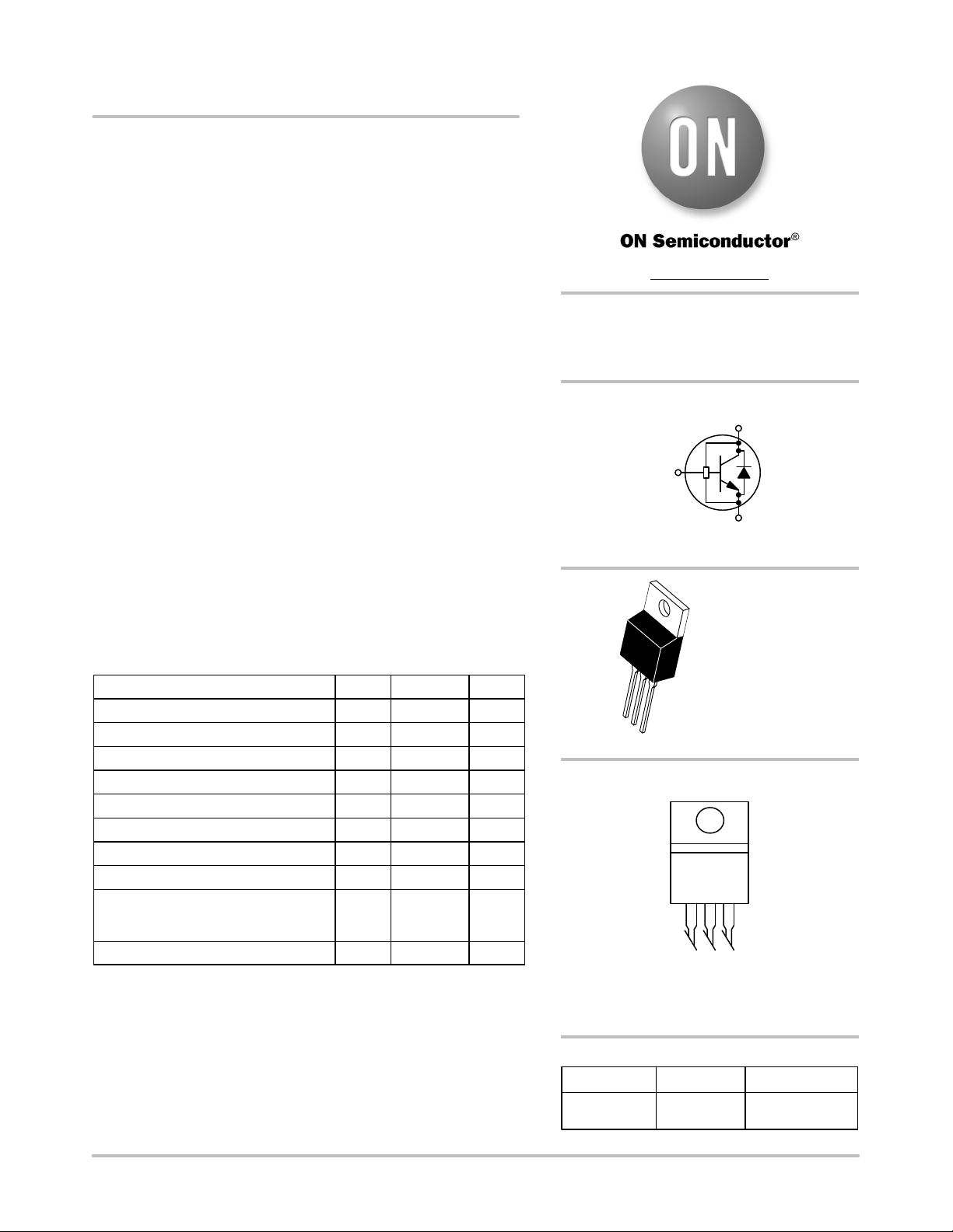
POWER TRANSISTOR
5.0 AMPERES,
700 VOLTS, 75 WATTS
TO−220
CASE 221A
STYLE 1
1
www.onsemi.com
MARKING DIAGRAM
2
3
BUL45D2G
AY WW
A = Assembly Location
Y = Year
WW = Work Week
G = Pb−Free Package
Device Package Shipping
ORDERING INFORMATION
BUL45D2G TO−220
(Pb−Free)
50 Units / Rail
1
BASE
3
EMITTER
COLLECTOR
2, 4
4
Verzeichnis