


herunterladen

LM2577 Three Output,
Isolated Flyback Regulator
Many voltage regulator applications require multiple outputs,
such as a computer’s power supply or a regulator used to
meet the voltage requirements inside an automobile. Some
of these applications require isolation between the regula-
tor’s input and output for protection and separate ground
specifications. Using this criteria, a LM2577 simple switcher
flyback regulator hasbeen designed with multiple (3) outputs
and input-to-output isolation. The three outputs are: 1) 5V
@
150 mA, 2) 7.5V
@
100 mA, and 3) −7.5V
@
70 mA. The
table below gives the electrical specifications.
The LM2577 flyback regulator uses a 4N27 optocoupler to
provide a galvanic isolation. The base resistor of the opto-
coupler is chosen so that it is large enough (47 kΩ) to supply
a minimum base current—which in turn, demands a lower
drive current to the optocoupler’sdiode— but not so large as
to produce a pole in the regulator’s frequency response. If
the pole’s frequency is below the regulator loop’s crossover
frequency, stability problems will occur. Thus, a zero must be
developed, requiring extra circuitry, to compensate for the
extra pole in the loop.
An LM385 Adjustable Voltage Reference, along with resis-
tors R
O1
and R
O2
, set the main output voltage to 5V
±
4
%
by
the equation: V
O
=
1.24V (1 + R
O2
/R
O1
). The LM385 sup-
plies a drive current to the optocoupler (about 10 mA) pro-
portional to the output voltage. Due to the high gain of the
LM385, the LM2577’s error amplifier is bypassed, and the
feedback signal is fed directly to the compensation pin. Em-
ploying the error amplifier’s gain block in the loop would add
with the LM385 gain (the optocoupler’s gain is around unity)
to produce a very large overall loop gain. Such a large loop
gain makes the loop too difficult to stabilize—thus the by-
passed error amplifier. With the regulator input voltage of
26V and full load on all outputs, the frequency response has
a crossover frequency at 1 kHz and phase margin of 90˚.
The flyback regulator’s modeof operation is continuous, so a
large primary inductance (L
P
=
300 µH) is needed for the
transformer. Using a Ferroxcube 812E250-3C8 E core, the
primary winding requires about 50 turns. With the turnsratios
as they are shown on the schematic and the small core size,
the transformer windings must be wound tightly so that they
fit the core windows. Interlaying the primary winding be-
tween the secondary windings improves the transformers
coupling.
The zener diode circuit (V
Z
,R
Z
,R
I
) is added to provide the
optocoupler transistor with about 20 µA of bias current, on
top of the current sourced from the compensation pin (about
7 µA). The isolation resistor, between the compensation pin
and the zener diode, needs to be as large as 100 kΩ,orat
start-up, the compensation pin will see too large a voltage,
turning the power switch fully on— thus forcing the LM2577
into current limit.Also, to ensure good line regulation, the dy-
namic impedance of the zener diode must be very good.
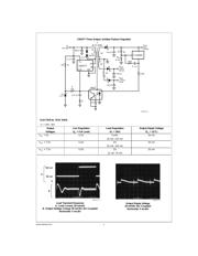
Test data for thisregulator follows the schematic. Since feed-
back is taken from Output 1, its load and line regulation are
better than that of the other two outputs, which rely on feed-
back through the transformer coupling. The output ripple
voltage of all three outputs is largely dependent on the filter
capacitors used, and could be reduced by the use of addi-
tional high-quality filter capacitors or an additional L-C filter
section.
National Semiconductor
Application Note 777
Tom Gross
April 1998
LM2577 Three Output, Isolated Flyback Regulator AN-777
© 1998 National Semiconductor Corporation AN011217 www.national.com