
herunterladen
© Semiconductor Components Industries, LLC, 2009
October, 2009− Rev. 7
1 Publication Order Number:
CS5253B−8/D
CS5253B-8
3.0 A LDO 5-Pin 2.5 V Fixed
Linear Regulator for
Remote Sense Applications
This new very low dropout linear regulator reduces total power
dissipation in the application. To achieve very low dropout, the
internal pass transistor is powered separately from the control
circuitry. Furthermore, with the control and power inputs tied together,
this device can be used in single supply configuration and still offer a
better dropout voltage than conventional PNP−NPN based LDO
regulators. In this mode the dropout is determined by the minimum
control voltage.
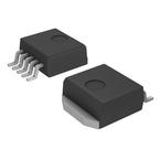
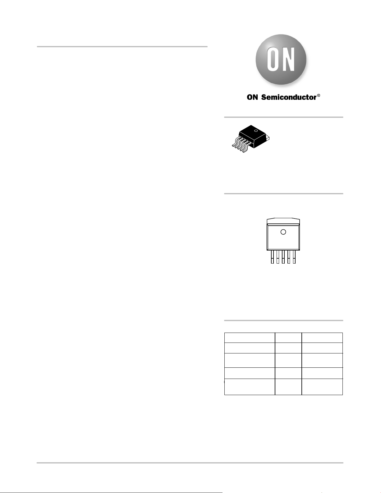
The CS5253B−8 is offered in a five−terminal D
2
PAK−5 package,
which allows for the implementation of a remote−sense pin permitting
very accurate regulation of output voltage directly at the load, where it
counts, rather than at the regulator. This remote sensing feature
virtually eliminates output voltage variations due to load changes and
resistive voltage drops. Typical load regulation measured at the sense
pin is less than 1.0 mV for an output voltage of 2.5 V with a load step
of 10 mA to 3.0 A.
The CS5253B−8 has a very fast transient loop response.
Internal protection circuitry provides for “bust−proof” operation,
similar to three−terminal regulators. This circuitry, which includes
overcurrent, short circuit, and overtemperature protection will self
protect the regulator under all fault conditions.
The CS5253B−8 is ideal for generating a 2.5 V supply to power
graphics controllers used on VGA cards. Its remote sense and low
value capacitance requirements make this a low cost high performance
solution. The CS5253B−8 is optimized from the CS5253−1 to allow a
lower value of output capacitor to be used at the expense of a slower
transient response.
Features
• V
OUT
Fixed @ 2.5 V ± 1.5%
• V
POWER
Dropout < 0.40 V @ 3.0 A
• V
CONTROL
Dropout < 1.05 V @ 3.0 A
• 1.5% Trimmed Reference
• Fast Transient Response
• Remote Voltage Sensing
• Thermal Shutdown
• Current Limit
• Short Circuit Protection
• Drop−In Replacement for EZ1582
• Backwards Compatible with 3−Pin Regulators
• Very Low Dropout Reduces Total Power Consumption
• Pb−Free Packages are Available*
*For additional information on our Pb−Free strategy and soldering details, please
download the ON Semiconductor Soldering and Mounting Techniques
Reference Manual, SOLDERRM/D.
http://onsemi.com
MARKING DIAGRAM
CS5253B−8 = Device Code
A = Assembly Location
WL = Wafer Lot
Y = Year
WW = Work Week
G = Pb−Free Package
D
2
PAK−5
DP SUFFIX
CASE 936AC
1
5
CS
5253B−8
AWLYWWG
1
Tab = V
OUT
Pin 1. V
SENSE
2. GND
3. V
OUT
4. V
CONTROL
5. V
POWER
Device Package Shipping
†
ORDERING INFORMATION
CS5253B−8GDP5 D
2
PAK−5 50 Units/Rail
CS5253B−8GDPR5 D
2
PAK−5 750/Tape & Reel
†For information on tape and reel specifications,
including part orientation and tape sizes, please
refer to our Tape and Reel Packaging Specifications
Brochure, BRD8011/D.
CS5253B−8GDPR5G D
2
PAK−5
(Pb−Free)
750/Tape & Reel
CS5253B−8GDP5G D
2
PAK−5
(Pb−Free)
50 Units/Rail
Verzeichnis
- ・ Konfiguration des Pinbelegungsdiagramms on Seite 3
- ・ Abmessungen des Paketumrisses on Seite 8
- ・ Paket-Footprint-Pad-Layout on Seite 8
- ・ Teilenummerierungssystem on Seite 1 Seite 9
- ・ Markierungsinformationen on Seite 1
- ・ Blockdiagramm on Seite 3
- ・ Technische Daten on Seite 1
- ・ Anwendungsbereich on Seite 1 Seite 6
- ・ Elektrische Spezifikation on Seite 2 Seite 3 Seite 4