


herunterladen

Maxim > Design Support > Technical Documents > Application Notes > Battery Management > APP 221
Keywords: battery monitor, battery protector, product comparison, DS2760, DS2761, battery monitoring,
protection
APPLICATION NOTE 221
DS276x Product Comparison
Sep 10, 2002
Abstract: This application note describes the differences between the DS2760 battery monitor and
protector and the DS2761 battery monitor and protector. It describes each difference in detail and
indicates what, if any, changes would be required to an existing design to switch between the DS2760
and its predecessor, the DS2761.
Introduction
The DS2762, DS2761, and DS2760 die revision C2 provide upgrades to the operation of the original
DS2760 (die revisions B2 and B3). The differences among these devices are minor and can cause
confusion as to whether or not system hardware and software updates are needed to transition use from
one to another. Table 1 summarizes the functional differences among all DS276x devices.
Table 1. Summary of Device Differences
Feature DS2760B2/DS2760B3 DS2760C2 DS2761 DS2762
Low-Voltage Recovery √ √ √
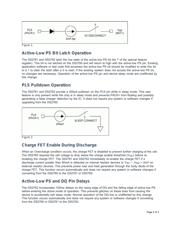
Active-Low PS Latch
√ √
PLS Pulldown
√ √
Charge FET Enable During Discharge
√ √
Active-Low
PS and DQ Delays √
Threshold Alarms
√
Increased ESD
Immunity √
Power-Up State Undefined SLEEP SLEEP ACTIVE
Low-Voltage Recovery Operation
The DS2760C2, DS2761, and DS2762 provide a maximum 10mA (2mA typical) charge path from the
PLS pin to the VDD pin. A depleted cell can be charged through this path to a point sufficient to power
the chip and allow normal charge. This path operates in parallel with any external charge path and
otherwise does not affect normal operation of the IC. The cell cannot be discharged through the recovery
path by pulling PLS low. Low-voltage recovery is disabled above 3.0V to prevent cell overcharge.
Page 1 of 3