

herunterladen
Semiconductor Components Industries, LLC, 2011
November, 2011 − Rev. 7
1 Publication Order Number:
DTA114EET1/D
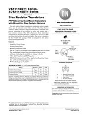
DTA114EET1 Series,
SDTA114EET1 Series
Preferred Devices
Bias Resistor Transistors
PNP Silicon Surface Mount Transistors
with Monolithic Bias Resistor Network
This new series of digital transistors is designed to replace a single
device and its external resistor bias network. The Bias Resistor
Transistor (BRT) contains a single transistor with a monolithic bias
network consisting of two resistors; a series base resistor and a
base−emitter resistor. The BRT eliminates these individual
components by integrating them into a single device. The use of a BRT
can reduce both system cost and board space. The device is housed in
the SC−75/SOT−416 package which is designed for low power
surface mount applications.
Features
Simplifies Circuit Design
Reduces Board Space
Reduces Component Count
The SC−75/SOT−416 package can be soldered using wave or reflow.
The modified gull−winged leads absorb thermal stress during
soldering eliminating the possibility of damage to the die.
AEC−Q101 Qualified and PPAP Capable
S Prefix for Automotive and Other Applications Requiring Unique
Site and Control Change Requirements
Pb−Free Packages are Available*
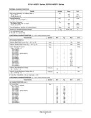
MAXIMUM RATINGS (T
A
= 25C unless otherwise noted)
Rating
Symbol Value Unit
Collector-Base Voltage V
CBO
50 Vdc
Collector-Emitter Voltage V
CEO
50 Vdc
Collector Current I
C
100 mAdc
Stresses exceeding Maximum Ratings may damage the device. Maximum
Ratings are stress ratings only. Functional operation above the Recommended
Operating Conditions is not implied. Extended exposure to stresses above the
Recommended Operating Conditions may affect device reliability.
*For additional information on our Pb−Free strategy and soldering details, please
download the ON Semiconductor Soldering and Mounting Techniques
Reference Manual, SOLDERRM/D.
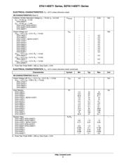
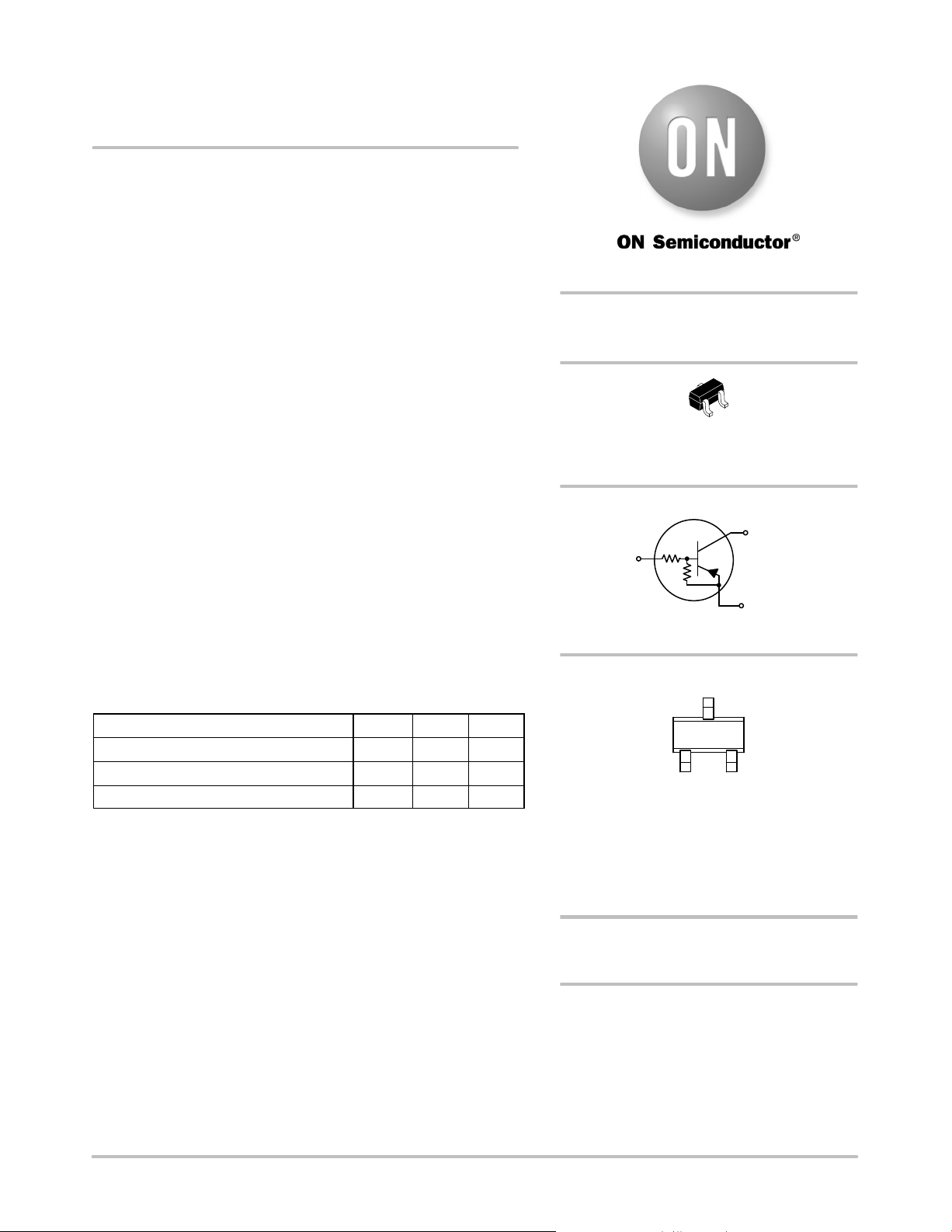
SC−75 (SOT−416)
CASE 463
STYLE 1
Preferred devices are recommended choices for future use
and best overall value.
PNP SILICON BIAS
RESISTOR TRANSISTORS
PIN 3
COLLECTOR
(OUTPUT)
PIN 2
EMITTER
(GROUND)
PIN 1
BASE
(INPUT)
R1
R2
MARKING DIAGRAM
xx M G
G
http://onsemi.com
See detailed ordering and shipping information in the package
dimensions section on page 4 of this data sheet.
ORDERING INFORMATION
xx = Specific Device Code
xx = (Refer to page 4)
M = Date Code*
G =Pb−Free Package
(Note: Microdot may be in either location)
*Date Code orientation may vary depending
upon manufacturing location.
Verzeichnis
- ・ Abmessungen des Paketumrisses on Seite 13
- ・ Paket-Footprint-Pad-Layout on Seite 13
- ・ Teilenummerierungssystem on Seite 1 Seite 4 Seite 13
- ・ Markierungsinformationen on Seite 1 Seite 4
- ・ Typisches Anwendungsschaltbild on Seite 10
- ・ Technische Daten on Seite 4
- ・ Anwendungsbereich on Seite 1
- ・ Elektrische Spezifikation on Seite 2 Seite 3 Seite 6 Seite 7 Seite 8