
herunterladen
This is preliminary information on a new product now in development or undergoing evaluation. Details are subject to
change without notice.
September 2013 Doc ID 18078 Rev 4 1/133
1
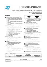
SPC564A70B4, SPC564A70L7
32-bit Power Architecture
®
based MCU for automotive
powertrain applications
Datasheet
−
preliminary data
Features
■
150 MHz e200z4 Power Architecture
®
core
– Variable length instruction encoding (VLE)
– Superscalar architecture with 2 execution
units
– Up to 2 integer or floating point instructions
per cycle
– Up to 4 multiply and accumulate operations
per cycle
■
Memory organization
– 2 MB on-chip flash memory with ECC and
read-while-write (RWW)
– 128 KB on-chip SRAM with standby
functionality (32 KB) and ECC
– 8 KB instruction cache (with line locking),
configurable as 2- or 4-way
– 14 + 3 KB eTPU code and data RAM
–4 × 4 crossbar switch (XBAR)
– 24-entry MMU
■
Fail Safe Protection
– 16-entry Memory Protection Unit (MPU)
– CRC unit with 3 submodules
– Junction temperature sensor
■
Interrupt
– Configurable interrupt controller (INTC)
with non-maskable interrupt (NMI)
– 64-channel eDMA
■
Serial channels
– 3 eSCI modules
– 3 DSPI modules (2 of which support
downstream Micro Second Channel [MSC])
– 3 FlexCAN modules with 64 message
buffers each
– 1 FlexRay module (V2.1) up to 10 Mbit/s
w/dual or single channel, 128 message
objects, ECC
■
1 eMIOS (24 unified channels)
■
1 eTPU2 (second generation eTPU)
– 32 standard channels
– 1 reaction module (6 channels with 3
outputs per channel)
■
2 enhanced queued analog-to-digital
converters (eQADCs)
– Forty 12-bit input channels
– 688 ns minimum conversion time
■
On-chip CAN/SCI Bootstrap loader with Boot
Assist Module (BAM)
■
Nexus: Class 3+ for core; Class 1 for eTPU
■
JTAG (5-pin)
■
Development Trigger Semaphore (DTS)
■
Clock generation
– On-chip 4–40 MHz main oscillator
– On-chip FMPLL (frequency-modulated
phase-locked loop)
■
Up to 112 general purpose I/O lines
■
Power reduction modes: slow, stop, and
standby
■
Flexible supply scheme
– 5 V single supply with external ballast
– Multiple external supply: 5 V, 3.3 V , and
1.2 V
■
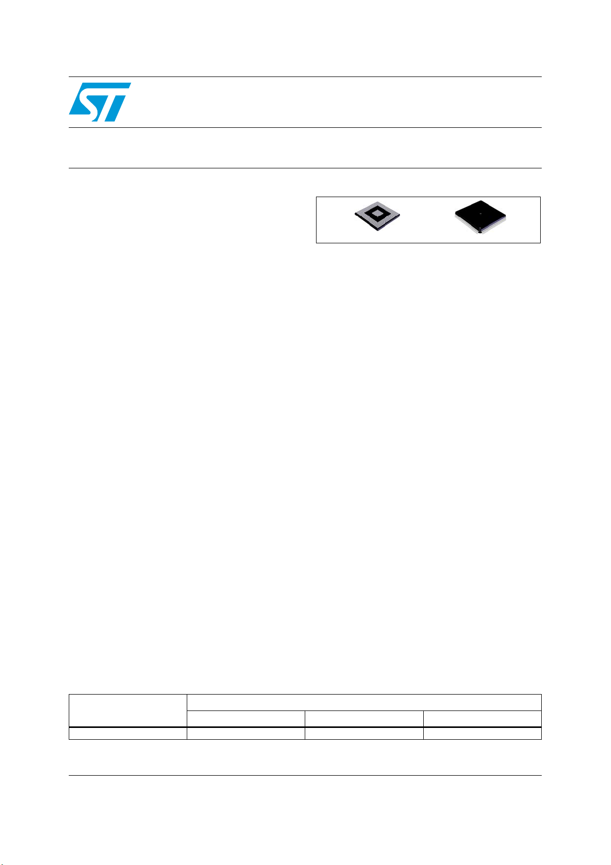
Designed for LQFP176, LBGA208, PBGA324
PBGA324 (23 mm x 23 mm)
LQFP176 (24 mm x 24 mm)
Table 1. Device summary
Memory Flash size
Part number
Package LQFP176 Package LBGA208 Package PBGA324
2MB SPC564A70L7 - SPC564A70B4
www.st.com
Verzeichnis