


herunterladen
© Semiconductor Components Industries, LLC, 2008
December, 2016 − Rev. 2
1 Publication Order Number:
AND8308/D
AND8308/D
Interpretation of Datasheet
Parameters for ESD
Devices
Introduction
Electrostatic Discharge (ESD) protection devices play an
important role in protecting electronic products from surges
and ESD events. The selection of the proper ESD device for
a given application requires an understanding of both the
system that needs protection as well as an understanding of
the properties of the ESD diode. The ESD device must not
disrupt the functionality of the system it is protecting during
normal operation but also must react quickly to shunt
dangerous current and voltage spikes to ground during surge
and ESD events.
This application note will define the parameters that can
be found on ESD/TVS protection diodes’ datasheets and
explain the relevance of each parameter.
DC Parameters
The key DC parameters of an ESD diode are presented
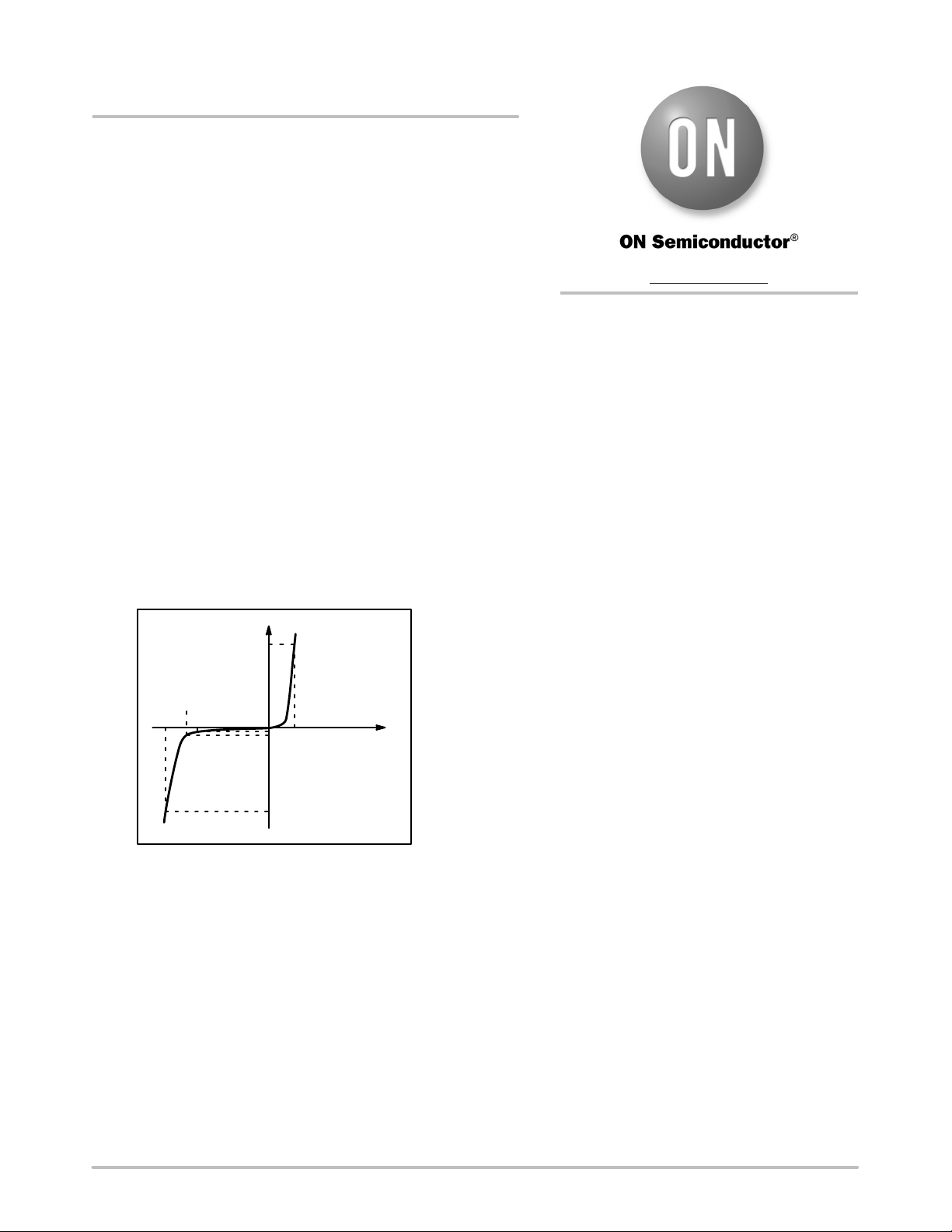
below. A typical IV characteristic curve for a unidirectional
ESD diode is shown in Figure 1.
Figure 1. Unidirectional IV Characteristic Curve
of an ESD and TVS
V
BR
= Breakdown Voltage @ I
T
V
RWM
= Reverse Working Voltage
@ I
R
(V
RWM
(typ) = 0.8 x V
BR
)
I
T
= Test Current
I
PP
= Maximum Reverse
Peak Pulse Current (Typically
Specified with either the
8x20 ms or 10x1000 ms Surge
Pulse)
V
C
= Clamping Voltage @ I
PP
V
C
V
BR
V
RWM
V
I
I
PP
I
T
I
R
Reverse Working Voltage, V
RWM
: Maximum nominal
working voltage for which the ESD device is intended for
use. At this voltage, the ESD diode will appear in the “off”
state as a high impedance element that will have very low
leakage current. The V
RWM
is below the reverse breakdown
voltage, V
BR
.
Reverse Breakdown Voltage, V
BR
: At this voltage, the
ESD diode starts to conduct, or turn “on”. The breakdown
is measured at a test current, I
T
, typically from 1mA to
10 mA. V
BR
is specified as a minimum value for ESD
applications and usually is 10% to 15% above the V
RWM
.
When selecting an ESD protection diode a designer must
ensure that this voltage is higher than the maximum working
voltage of the system it is protecting.
Forward Voltage, V
F
: Voltage in the forward direction at
the test current, I
F
.
Capacitance, C: Capacitance is a parameter that becomes
a concern for applications that operate at high data rates.
High capacitance will degrade signals, compromising high
speed applications. A device with low capacitance is
preferred for high speed applications. HDMI and USB
connections are examples of high speed applications where
low capacitance is needed.
ESD and Surge Parameters
Interpretation of clamping specs during ESD or transient
events is commonly misunderstood on ESD protection
datasheets. There is no industry recognized standard for
specifying clamping performance of ESD protection diodes
and it is highly dependant on the testing conditions and input
waveforms.
Survivability Specs
Peak Pulse Current, I
PP
: Maximum surge current which
the device can withstand without damage. Most low power
TVS diodes are specified with the 8 ms x 20 ms current surge
pulse. Higher power TVS diodes are measured with the
10 ms x 1000 ms current surge pulse. See Figures 2 and 3 for
definitions of these waveforms. This parameter plays an
important role to determine the robustness for high power
transient voltage suppression (TVS) applications such as
lightning or inductive switching applications, but is not as
crucial for applications that are predominantly concerned
with ESD events such as portables applications.
APPLICATION NOTE
www.onsemi.com
Verzeichnis