


January 2013
© 2012 Fairchild Semiconductor Corporation www.fairchildsemi.com
FAN302HLMY_F117 • Rev. 1.0.2
FAN302HLMY_F117 — mWSaver™ PWM Controller for Low Standby Power Battery-Charger Applications
FAN302HLMY_F117
PWM Controller for Low Standby Power Battery-
Charger Applications — mWSaver™ Technology
Features
mWSaver™ Technology Provides Industry’s
Best-in-Class Standby Power
- Ultra Low Power Consumption at No Load
(<10 mW at 230 V
AC
)
- Proprietary 500V High-Voltage JFET Startup
Reduces Startup Resistor Loss
- Low Operation Current in Burst Mode:
350 µA Maximum
Constant-Current (CC) Control without Secondary-
Feedback Circuitry
Fixed PWM Frequency at 85kHz with Frequency
Hopping to Reduce EMI
High-Voltage Startup
Low Operating Current: 3.5 mA
Peak-Current-Mode Control with Slope
Compensation
Cycle-by-Cycle Current Limiting
V
DD
Over-Voltage Protection (Auto-Restart)
V
S
Over-Voltage Protection (Latch Mode)
V
DD
Under-Voltage Lockout (UVLO)
Gate Output Maximum Voltage Clamped at 15 V
Fixed Over-Temperature Protection (Latch Mode)
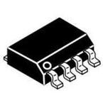
Available in an 8-Lead SOIC Package
Applications
Battery Chargers for Cellular Phones, Cordless
Phones, PDAs, Digital Cameras, and Power Tools
Replaces Linear Regulators and RCC SMPS
Description
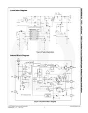
The FAN302HLMY_F117 advanced PWM controller
significantly simplifies isolated power supply design that
requires CC regulation of the output. The output current
is precisely estimated with information in the primary
side of the transformer and controlled with an internal
compensation circuit. This removes the output current
sensing loss and eliminates all external Control Circuitry
(CC). The Green-Mode function, with an extremely low
operating current (200 µA) in Burst Mode, maximizes
the light-load efficiency, enabling conformance to
worldwide Standby Mode efficiency guidelines.
Integrated protections include two-level pulse-by-pulse
current limit, Over-Voltage Protection (OVP), brownout
protection, and Over-Temperature Protection (OTP).
Compared with a conventional approach using an
external control circuit in the secondary side for CC
regulation, the FAN302HLMY_F117 can reduce total
cost, component count, size, and weight; while
simultaneously increasing efficiency, productivity, and
system reliability.
Figure 1. Typical Output V-I Characteristic
Ordering Information
Part Number
Operating
Temperature Range
Package
Packing
Method
FAN302HLMY_F117
-40°C to +105°C
8-Lead, Small Outline Package (SOIC),
JEDEC MS-012, .150-Inch Narrow Body
Tape & Reel
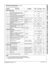
I
O
V
O
Maximum
Typical
Minimum
Verzeichnis
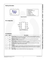
- ・ Konfiguration des Pinbelegungsdiagramms on Seite 3
- ・ Abmessungen des Paketumrisses on Seite 18
- ・ Paket-Footprint-Pad-Layout on Seite 18
- ・ Teilenummerierungssystem on Seite 1
- ・ Markierungsinformationen on Seite 3
- ・ Blockdiagramm on Seite 2 Seite 16
- ・ Typisches Anwendungsschaltbild on Seite 2 Seite 16 Seite 17
- ・ Schweißen Temperatur on Seite 4
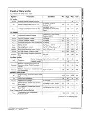
- ・ Technische Daten on Seite 4 Seite 17
- ・ Anwendungsbereich on Seite 1 Seite 2 Seite 3 Seite 4 Seite 5
- ・ Elektrische Spezifikation on Seite 5 Seite 6 Seite 7 Seite 8 Seite 9