


herunterladen

MMG3003NT1
1
RF Device Data
Freescale Semiconductor, Inc.
MMG3003NT1
40--3600 MHz, 20 dB
24 dBm
InGaP HBT GPA
Heterojunction Bipolar Transistor
Technology (InGaP HBT)
Broadband High Linearity Amplifier
The MMG3003NT1 is a general purpose amplifier that is internally input
matched and internally output prematched. It is designed for a broad range
of Class A, small --signal, high linearity, general purpose applications. It is
suitable for applications with frequencies from 40 to 3600 MHz such as
cellular, PCS, BWA, WLL, PHS, CATV, VHF, UHF, UMTS and general
small--signal RF.
Features
Frequency: 40--3600 MHz
P1dB: 24 dBm @ 900 MHz
Small--Signal Gain: 20 dB @ 900 MHz
Third Order Output Intercept Point: 40.5 dBm @ 900 MHz
Single Voltage Supply
Internally Matched to 50 Ohms
Cost--effective SOT--89 Surface Mount Plastic Package
In Tape and Reel. T1 Suffix = 1,000 Units, 12 mm Tape Width, 7--inch Reel.
SOT--89
Table 1. Typical Performance
(1)
Characteristic Symbol
900
MHz
2140
MHz
3500
MHz
Unit
Small--Signal Gain
(S21)
G
p
20 16.9 12 dB
Input Return Loss
(S11)
IRL -- 1 5 --14.1 -- 11 . 2 dB
Output Return Loss
(S22)
ORL -- 9 . 3 --14.5 --10.2 dB
Power Output @1dB
Compression
P1dB 24 23.3 20.5 dBm
Third Order Output
Intercept Point
OIP3 40.5 40 37 dBm
1. V
CC
=6.2Vdc,T
A
=25C, 50 ohm system.
Table 2. Maximum Ratings
Rating Symbol Value Unit
Supply Voltage V
CC
7 V
Supply Current I
CC
400 mA
RF Input Power P
in
15 dBm
Storage Temperature Range T
stg
--65 to +150 C
Junction Temperature T
J
175 C
Table 3. Thermal Characteristics
Characteristic Symbol Value
(2)
Unit
Thermal Resistance, Junction to Case
Case Temperature 109C, 6.2 Vdc, 180 mA, no RF applied
R
JC
31.6 C/W
2. Refer to AN1955, Thermal Measurement Methodology of RF Power Amplifiers. Go to http://www.freescale.com/rf.
Select Documentation/Application Notes -- AN1955.
Document Number: MMG3003NT1
Rev. 9, 9/2014
Freescale Semiconductor
Technical Data
Freescale Semiconductor, Inc., 2004--2008, 2012, 2014.
A
ll rights reserved.
Verzeichnis
- ・ Konfiguration des Pinbelegungsdiagramms on Seite 2
- ・ Abmessungen des Paketumrisses on Seite 13
- ・ Paket-Footprint-Pad-Layout on Seite 12
- ・ Markierungsinformationen on Seite 12
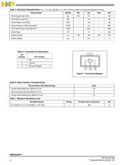
- ・ Blockdiagramm on Seite 5 Seite 6 Seite 7 Seite 8 Seite 9
- ・ Typisches Anwendungsschaltbild on Seite 2
- ・ Technische Daten on Seite 1
- ・ Elektrische Spezifikation on Seite 2