
herunterladen

1
INDUSTRIAL TEMPERATURE RANGE
IDT5V9885
3.3V EEPROM PROGRAMMABLE CLOCK GENERATOR
OCTOBER 2007
2007 Integrated Device Technology, Inc. DSC 6787/39c
IDT5V9885
INDUSTRIAL TEMPERATURE RANGE
3.3V EEPROM
PROGRAMMABLE CLOCK
GENERATOR
The IDT logo is a registered trademark of Integrated Device Technology, Inc.
FEATURES:
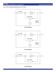
• Three internal PLLs
• Internal non-volatile EEPROM
• JTAG and FAST mode I
2
C serial interfaces
• Input Frequency Ranges: 1MHz to 400MHz
• Output Frequency Ranges: 4.9kHz to 500MHz
• Reference Crystal Input with programmable oscillator gain and
programmable linear load capacitance
−
Crystal Frequency Range: 8MHz to 50MHz
• Each PLL has an 8-bit pre-scaler and a 12-bit feedback-divider
• 10-bit post-divider blocks
• Fractional Dividers
• Two of the PLLs support Spread Spectrum Generation
capability
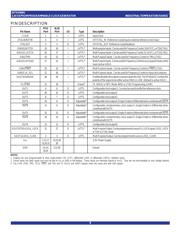
• I/O Standards:
−
Outputs - 3.3V LVTTL/ LVCMOS, LVPECL, and LVDS
−
Inputs - 3.3V LVTTL/ LVCMOS
• Programmable Slew Rate Control
• Programmable Loop Bandwidth Settings
• Programmable output inversion to reduce bimodal jitter
• Redundant clock inputs with glitchless auto and manual
switchover options
• JTAG Boundary Scan
• Individual output enable/disable
• Power-down mode
• 3.3V VDD
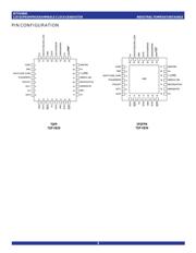
• Available in TQFP and VFQFPN packages
DESCRIPTION:
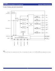
The IDT5V9885 is a programmable clock generator intended for high
performance data-communications, telecommunications, consumer, and
networking applications. There are three internal PLLs, each individually
programmable, allowing for three unique non-integer-related frequencies.
The frequencies are generated from a single reference clock. The
reference clock can come from one of the two redundant clock inputs. A
glitchless automatic or manual switchover function allows any one of the
redundant clocks to be selected during normal operation.
The IDT5V9885 can be programmed through the use of the I
2
C or JTAG
interfaces. The programming interface enables the device to be pro-
grammed when it is in normal operation or what is commonly known as in-
system programmable. An internal EEPROM allows the user to save and
restore the configuration of the device without having to reprogram it on
power-up. JTAG boundary scan is also implemented.
Each of the three PLLs has an 8-bit pre-scaler and a 12-bit feedback
divider. This allows the user to generate three unique non-integer-related
frequencies. The PLL loop bandwidth is programmable to allow the user
to tailor the PLL response to the application. For instance, the user can tune
the PLL parameters to minimize jitter generation or to maximize jitter
attenuation. Spread spectrum generation and fractional divides are
allowed on two of the PLLs.
There are 10-bit post dividers on five of the six output banks. Two of the
six output banks are configurable to be LVTTL, LVPECL, or LVDS. The
other four output banks are LVTTL. The outputs are connected to the PLLs
via the switch matrix. The switch matrix allows the user to route the PLL
outputs to any output bank. This feature can be used to simplify and optimize
the board layout. In addition, each output's slew rate and enable/disable
function can be programmed.