
herunterladen
1
FN9135.4
CAUTION: These devices are sensitive to electrostatic discharge; follow proper IC Handling Procedures.
1-888-INTERSIL or 1-888-468-3774
| Intersil (and design) is a registered trademark of Intersil Americas Inc.
Copyright © Intersil Americas Inc. 2003-2005. All Rights Reserved. Dynamic VID® is a registered trademark of Intersil Americas Inc.
All other trademarks mentioned are the property of their respective owners.
ISL6565A, ISL6565B
Multi-Phase PWM Controller with
Precision r
DS(ON)
or DCR Current Sensing
for VR10.X Application
The ISL6565A, ISL6565B controls microprocessor core
voltage regulation by driving up to 3 synchronous-rectified
buck channels in parallel. Multi-phase buck converter
architecture uses interleaved timing to multiply channel
ripple frequency and reduce input and output ripple currents.
The difference between the ISL6565A and the ISL6565B is
that the ISL6565A utilizes r
DS(ON)
current sensing, while the
ISL6565B utilizes DCR current sensing for each phase.
These cost and space saving methods of current sensing
are used for adaptive voltage positioning (droop), channel-
current balancing, and overcurrent protection. To ensure the
accuracy of droop, a programmable internal temperature
compensation function is implemented to compensate the
effect of r
DS(ON)
and DCR temperature sensitivity.
A unity gain, differential amplifier is provided for remote
voltage sensing. Any potential difference between remote
and local grounds is eliminated using the remote-sense
amplifier. The precision threshold-sensitive enable input is
available to accurately coordinate the start up of the
ISL6565A, ISL6565B with Intersil MOSFET driver ICs.
Dynamic-VID™ technology allows seamless on-the-fly VID
changes. The offset pin allows accurate voltage offset
settings that are independent of VID setting.
Features
• Multi-Phase Power Conversion
- 2 or 3 Phase Operation
• Precision Core Voltage Regulation
- Differential Remote Voltage Sensing
- 0.5% System Accuracy Over Temperature and Life
- Adjustable Reference-Voltage Offset
• Precision r
DS(ON)
or DCR Current Sensing
- Integrated Programmable Temperature Compensation
- Accurate Load-Line Programming
- Accurate Channel-Current Balancing
- Low-Cost, Lossless Current Sensing
• Input Voltage: 12V or 5V Bias
• Microprocessor Voltage Identification Input
- Dynamic VID® Technology
- 6-Bit VID Input
- 0.8375V to 1.600V in 12.5mV Steps
• Threshold Enable Function for Precision Sequencing
• Overcurrent Protection
• Overvoltage Protection
• Digital Soft-Start
• Operation Frequency up to 1.5MHz per Phase
• QFN Package
- Compliant to JEDEC PUB95 MO-220
QFN - Quad Flat No Leads - Package Outline
- Near Chip Scale Package Footprint, which Improves
PCB Efficiency and Has a Thinner Profile
• Pb-Free Plus Anneal Available (RoHS Compliant)
Ordering Information
PART NUMBER PART MARKING TEMP. RANGE (°C) PACKAGE PKG. DWG. #
ISL6565ACB ISL6565ACB 0 to 105 28 Ld SOIC M28.3
ISL6565ACBZ (Note) ISL6565ACBZ 0 to 105 28 Ld SOIC (Pb-free) M28.3
ISL6565ACR ISL6565ACR 0 to 105 28 Ld 5x5 QFN L28.5x5
ISL6565ACRZ (Note) ISL6565ACRZ 0 to 105 28 Ld 5x5 QFN (Pb-free) L28.5x5
ISL6565ACV ISL6565ACV 0 to 105 28 Ld TSSOP M28.173
ISL6565ACVZ (Note) ISL6565ACVZ 0 to 105 28 Ld TSSOP (Pb-free) M28.173
ISL6565BCB ISL6565BCB 0 to 105 28 Ld SOIC M28.3
ISL6565BCBZ (Note) ISL6565BCBZ 0 to 105 28 Ld SOIC (Pb-free) M28.3
ISL6565BCR ISL6565BCR 0 to 105 28 Ld 5x5 QFN L28.5x5
ISL6565BCRZ (Note) ISL6565BCRZ 0 to 105 28 Ld 5x5 QFN (Pb-free) L28.5x5
ISL6565BCV ISL6565BCV 0 to 105 28 Ld TSSOP M28.173
ISL6565BCVZ (Note) ISL6565BCVZ 0 to 105 28 Ld TSSOP (Pb-free) M28.173
*Add "-T" suffix for tape and reel.
NOTE: Intersil Pb-free plus anneal products employ special Pb-free material sets; molding compounds/die attach materials and 100% matte tin plate
termination finish, which are RoHS compliant and compatible with both SnPb and Pb-free soldering operations. Intersil Pb-free products are MSL
classified at Pb-free peak reflow temperatures that meet or exceed the Pb-free requirements of IPC/JEDEC J STD-020.
Data Sheet December 1, 2005
N
O
T
R
E
C
O
M
M
E
ND
E
D
F
O
R
N
E
W
D
E
S
I
G
NS
N
O
RE
C
O
M
M
E
N
D
E
D
R
E
P
L
A
C
E
M
E
N
T
c
o
n
t
a
c
t
o
u
r
T
e
c
h
n
i
c
a
l
S
u
p
p
o
r
t
C
e
n
t
e
r
a
t
1
-
8
8
8
-
I
N
T
E
R
S
I
L
o
r
w
w
w
.
i
n
t
e
r
s
il
.
c
o
m
/
t
s
c
Verzeichnis
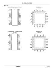
- ・ Konfiguration des Pinbelegungsdiagramms on Seite 9
- ・ Abmessungen des Paketumrisses on Seite 1
- ・ Teilenummerierungssystem on Seite 1
- ・ Markierungsinformationen on Seite 1
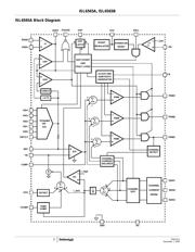
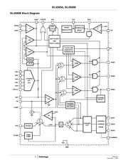
- ・ Blockdiagramm on Seite 3 Seite 4
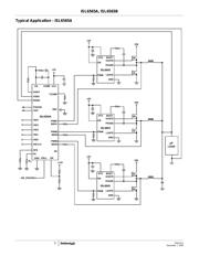
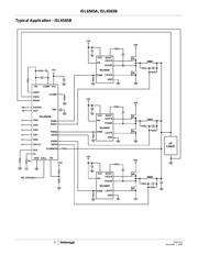
- ・ Typisches Anwendungsschaltbild on Seite 5 Seite 6 Seite 24
- ・ Technische Daten on Seite 8 Seite 16 Seite 18 Seite 23
- ・ Elektrische Spezifikation on Seite 8 Seite 16 Seite 18 Seite 23