


herunterladen

1
SNVA753–April 2016
Submit Documentation Feedback
Copyright © 2016, Texas Instruments Incorporated
LDOs Thermal Performance in Small SMD Packages
Application Report
SNVA753–April 2016
LDOs Thermal Performance in Small SMD Packages
AntonyCaravajales
ABSTRACT
This application report covers common questions regarding linear regulators and thermal metrics. This
document also compares continuous-load-condition and pulsed-load-condition thermal performance of low
dropout linear regulators (LDOs).
Contents
1 Purpose ....................................................................................................................... 3
2 Fundamentals ................................................................................................................ 3
3 Thermal Performance of SMD Packages................................................................................. 7
4 Frequently Asked Questions.............................................................................................. 14
5 TI Tools and Support ...................................................................................................... 16
Appendix A Evaluation Board Layers Stack and Layout Printout ......................................................... 17
Appendix B References......................................................................................................... 29
List of Figures
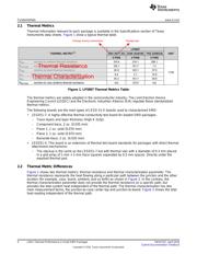
1 LP5907 Thermal Metrics Table ............................................................................................ 4
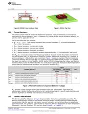
2 DSBGA Cross-Sectional View ............................................................................................. 4
3 DSBGA Top View............................................................................................................ 4
4 Thermal Resistance Comparison Between Packages.................................................................. 5
5 LP5907 DSBGA Package (R
θJA
= 206.1°C/W) ........................................................................... 8
6 LP5907 SOT Package (R
θJA
= 193.4°C/W) ............................................................................... 8
7 LP5907 X2SON Package (R
θJA
= 216.1°C/W)............................................................................ 8
8 LP5910 DSBGA Package (R
θJA
= 202.8°C/W) ........................................................................... 8
9 LP5910 WSON Package (R
θJA
= 79.2°C/W).............................................................................. 8
10 Comparison between JESD_M and JESD51-7 ........................................................................ 10
11 LP5907 DSBGA Board Comparison..................................................................................... 10
12 LP5910 Packages Comparison .......................................................................................... 11
13 SOT, SON, and BGA Package Thermal Response Comparison.................................................... 11
14 Load Pulse Duration 4s ................................................................................................... 12
15 Load Pulse Duration 400 ms ............................................................................................. 12
16 Load Pulse Duration 40 ms .............................................................................................. 12
17 Load Pulse Duration 4 ms ................................................................................................ 12
18 Transient Thermal Response Graph for LP5907 DSBGA ............................................................ 13
19 LP5900 WSON Layout .................................................................................................... 14
20 LP5900 Recommended Land Pattern .................................................................................. 15
21 JESD_M Layer Stackup................................................................................................... 17
22 JESD_M Top................................................................................................................ 17
23 JESD_M Signal Layer 1................................................................................................... 17
24 JESD_M Signal Layer 2................................................................................................... 17
25 JESD_M Bottom............................................................................................................ 17
26 JESD_H Layer Stackup ................................................................................................... 19
Verzeichnis
- ・ Technische Daten on Seite 4
- ・ Anwendungsbereich on Seite 30