

herunterladen
Click here for an overview of the wireless
components used in a typical radio
transceiver.
Maxim > Design Support > Technical Documents > Application Notes > Wireless and RF > APP 5417
Keywords: transmitter, receiver, ISM, RF, radio, PCB, antenna, impedance, range, matching, crystal, baseband, tuning, data rate, ASK, modulation
APPLICATION NOTE 5417
How to Optimize an ISM Radio Frequency (RF) System
By: Martin Stoehr, Principal Member of the Technical Staff, Applications
Oct 01, 2012
Abstract:
With industrial/scientific/medical (ISM) band
radio frequency (RF) products, often times users are new to the structure of Maxim's low pin-count transmitters and
fully integrated superheterodyne receivers. This tutorial provides simple steps that can be taken to get the best performance out of these transmitters and receivers while
providing techniques to measure the overall capability of the design.
A similar, Korean version of this article appears on EP&C News, September 6, 2012.
Introduction
Every day more industrial, scientific, and medical (ISM) band radio frequency (RF) products reach the marketplace. With so many
offerings available, it is not surprising that users are often unfamiliar with the structure of low-pin-count transmitters and fully integrated
superheterodyne receivers. This tutorial presents simple steps that designers can follow to achieve the best performance from these
transmitters and receivers. Techniques to measure the overall capability of these designs are also provided.
Transmitter Optimization
There are only two basic steps used to optimize the operation of a simple ISM transmitter (shown in Figure 1): make sure that the reference frequency is properly tuned,
and correctly match the output network of the transmitter to the antenna. A crystal oscillator is commonly used as the reference in both the transmitter and receiver circuits,
so that optimization technique is addressed in the Receiver Optimization section below.
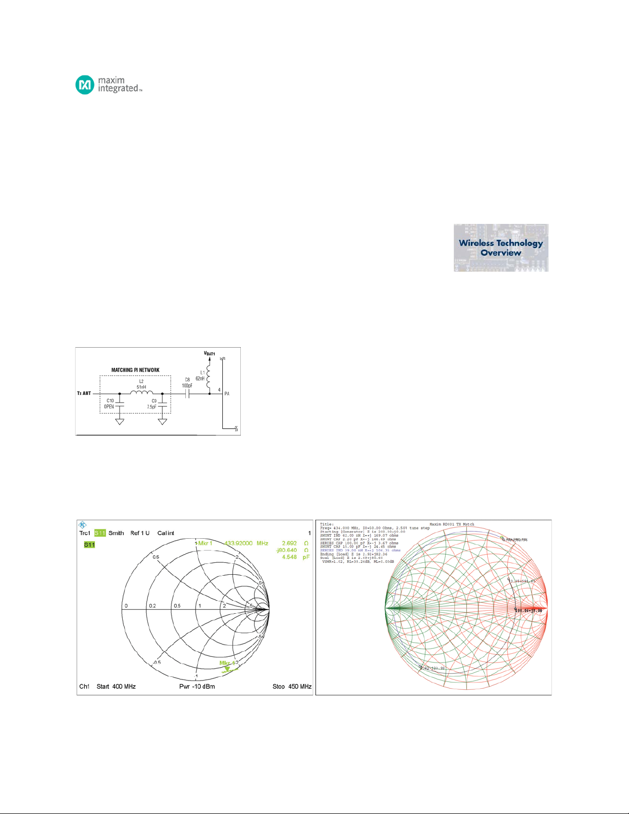
Figure 1. Basic ISM transmitter circuit.
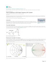
Matching the Transmitter (Tx) Antenna
For the initial matching of a Tx antenna, an S11 measurement (Figure 2A) is taken using a coax extension to the antenna feed point. The impedance transformation circuit
(Figure 1) was designed as a lowpass π network which accomplishes two things: first, it matches the power amplifier (PA) output impedance (modeled as 200Ω + j0) to the
complex conjugate of the antenna impedance (measured to be ~2.69Ω - j80.6 handheld, Figure 2, Figure 4); and second, it provides lowpass filtering to suppress
harmonics. In this instance, the value of the bias inductor for the PA is chosen to tune out the 2.0pF to 2.5pF stray capacitance to ground at the PA output. The series
capacitor, C8, serves as a DC block.
A B
Figures 2A and B. Measured impedance (A, top) and calculated network (B, bottom).
Page 1 of 7