


herunterladen
Keywords:
VCO, voltage controlled oscillators, Phase locked loop, PLL, LO, local oscillator, reference oscillator
APPLICATION NOTE 6269
UNDERSTANDING THE OPERATION OF THE FREQUENCY
SYNTHESIZER IN MAXIM’S RF TRANSCEIVERS
Abstract: The application note shows how to calculate the appropriate integer and fractional divider values for any desirable LO frequency that uses
different reference frequencies (i.e., 19.2MHz, 20.72 MHz, etc.). It tells the relationship between these two frequencies for five different Maxim’s RF
transceivers.
Introduction
All of Maxim's 2.4GHz to 6GHz highly integrated transceivers include a high performance fractional-N synthesizer for generating the local oscillator
(LO) signal. The fractional-N synthesizer generally consists of a phase locked loop with resolution as high as 20 bit, and integrated broadband voltage
controlled oscillators (VCO's). The only additional components needed to generate the high performance LO are the reference input and passive loop
filter. With the on-chip crystal oscillator, these transceivers can support both crystal and TCXO reference.
Traditional wireless data applications, such as Wi-Fi
and WiMAX , use 20MHz and 40MHz reference input; therefore, most of the control software
were designed with these default reference values. For applications that use different reference frequencies (i.e., 19.2MHz, 30.72MHz, etc.), users
must bypass the graphical interface of the control software and enter the appropriate integer and fractional divider values directly into the register table
for a given reference input frequency. This application note shows how to calculate the appropriate integer and fractional divider values for any
desirable LO frequency and reference frequency. It tells the relationship between these two frequencies for five different Maxim RF transceivers. The
specific frequency synthesizer parameters and register bits used to control these parameters are also shown. Every section is supported by an
example to show how the registers are set.
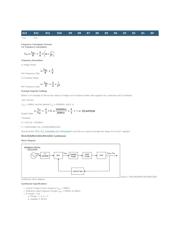
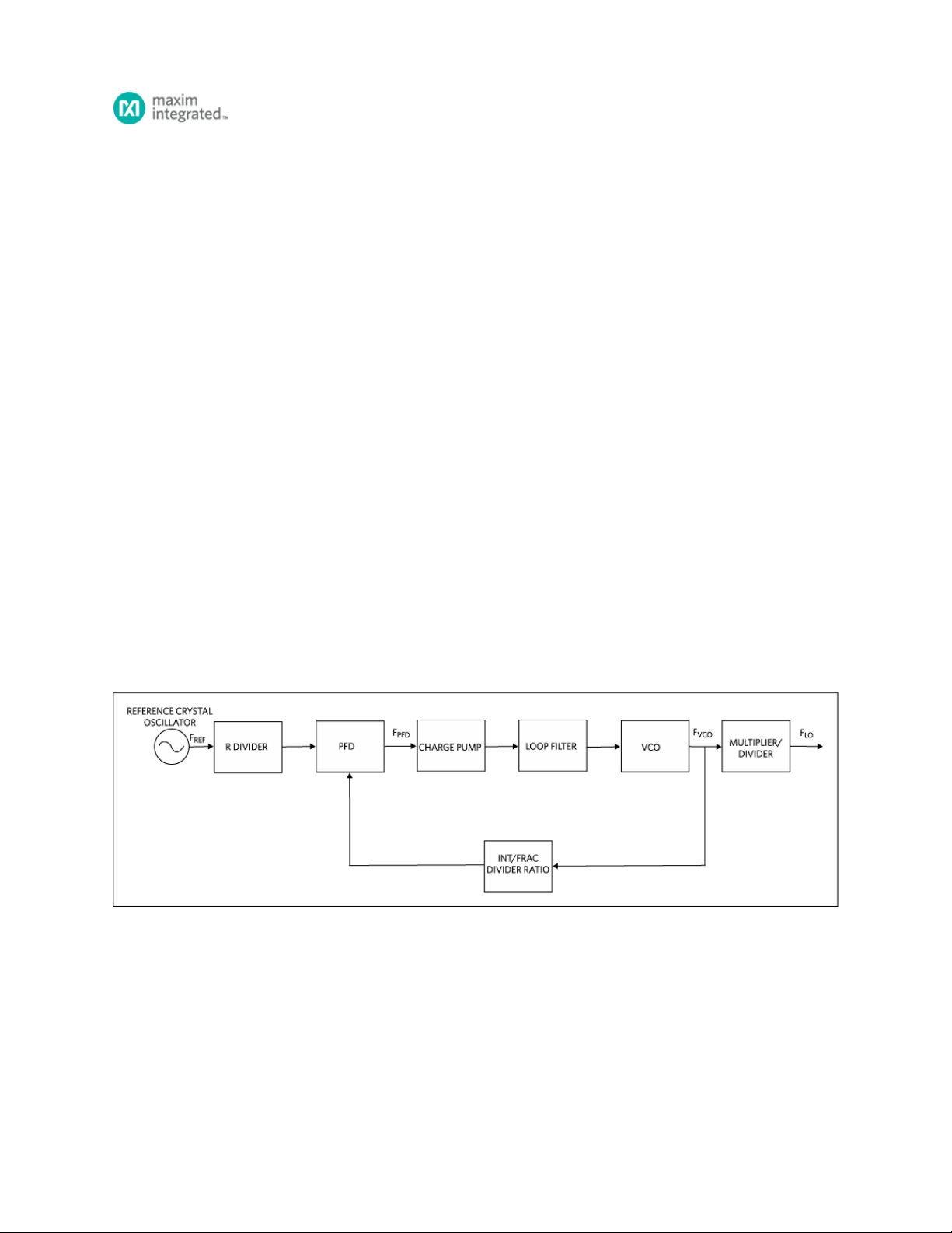
RF Synthesizer
Block Diagram
The RF frequency synthesizer is a negative feedback control system which consists of a reference, phase frequency
detector (PFD), charge pump,
loop
filter, voltage controlled oscillator (VCO), N counter, and RF output divider/multiplier (Figure 1). The high frequency VCO tracks the stable low
frequency reference in frequency and phase by comparing the divided down VCO output to the reference input through the PFD. The output of the
PFD is fed into the charge pump which then generates a current output proportional to the error. The current is converted into a voltage with the help
of the loop filter, which then modulates the tune voltage of the VCO. Lastly to mitigate VCO pulling, there are usually multipliers and dividers between
the VCO output and LO input to the mixers.
Figure 1. Frequency synthesizer block diagram.
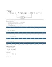
MAX2829 Synthesizer
Block Diagram
® ®
By: Wafa Iqbal
Verzeichnis