
herunterladen

Keywords: Battery Backup, Li+ Rechargeable cell, +5V, boost converter, battery charger
APPLICATION NOTE 5818
GET A CONSTANT +5V OUTPUT BY SWITCHING
BETWEEN A +5V INPUT AND A SINGLE-CELL
LI+ RECHARGEABLE CELL
By: Don Corey, Principal Member of Technical Staff, Maxim Integrated
Abstract: Design provides a simple method for maintaining an uninterrupted +5V even while switching
between the external +5V supply and a rechargeable single-cell Li+ battery.
Some portable applications need to be powered up from an external +5V wall adapter supply and still
require a +5V system voltage when in battery-backup mode. This design provides a simple method of
switching between the external +5V supply and a rechargeable single-cell Lithium-ion (Li+) battery. The
design will still maintain uninterrupted +5V to the application circuitry.
Three key circuit functions are needed:
1. An efficient Li+ battery charger
2. An efficient boost converter to convert the battery voltage to +5V
3. A low-loss switchover circuit that automatically switches between the main DC power and the backup
Li+ battery
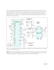
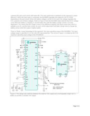
As shown in Figure 1, U1 is a high-performance battery charger (MAX8903) capable of supplying up to 2A
to charge a single-cell battery. Resistors RIDC and RISET set the DC-input current limit and charge-current
set points, respectively. Since the SYS output (pins 23 and 24) is not used, the charge current will be
constant and not dictated by the load current.
Q1 and Q2 are dual PNP transistors, available in an SC74 package. These transistors are used with the p-
channel FETs, Q4a and Q4b, to form ideal low-loss ORing diodes. The output of the ORing diode
configuration is then fed to a high-efficiency boost converter, U2 (MAX8815A). When the +5V input voltage
is present, the MAX8903 is charging the battery. Q4a conducts, as the voltage on R2 provides a negative
bias with respect to the Q4a source voltage. The voltage on the base of Q2b is higher than the voltage on
the emitter of Q2a transistor. Consequently, Q2a is turned off and Q2b is turned on because enough base
current flows thru R3 to ground. Since Q2b is now fully on, the voltage at the Q2b collector is very close to
the output voltage. Q4b is also biased off, as the voltage difference between its gate and source pins are
close to zero. When the +5V source is removed or lower than the battery voltage, circuit operation is
identical to the above description for Q4b, Q1a, Q1b, R4, and R1.
The MAX8815A (U2) is a highly efficient boost converter that delivers over 1A of continuous current. As the
input voltage to the MAX8815A has a range of 3.0V to 5V, this boost converter still provides a highly
regulated 5V output even when the input is +5V.
1
Page 1 of 4