
herunterladen
© Semiconductor Components Industries, LLC, 2014
April, 2014 − Rev. 13
1 Publication Order Number:
MC100EP40/D
MC100EP40
3.3V / 5V ECL Differential
Phase-Frequency Detector
Description
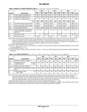
The MC100EP40 is a three−state phase−frequency detector
intended for phase−locked loop applications which require a minimum
amount of phase and frequency difference at lock. Advanced design
significantly reduces the dead zone of the detector. For proper
operation, the input edge rate of the R and V inputs should be less than
5 ns. The device is designed to work with a 3.3 V / 5 V power supply.
When Reference (R) and Feedback (FB) inputs are unequal in
frequency and/or phase the differential UP (U) and DOWN (D)
outputs will provide pulse streams which when subtracted and
integrated provide an error voltage for control of a VCO.
When Reference (R) and Feedback (FB) inputs are 80 ps or less in
phase difference, the Phase Lock Detect pin will indicate lock by a
high state (V
OH
). The V
TX
(V
TR
, V
TR
, V
TFB
, V
TFB
) pins offer an
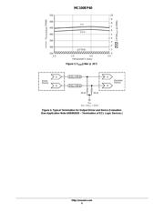
internal termination network for 50 W line impedance environment
shown in Figure 2. An external sinking supply of V
CC
−2 V is required
on V
TX
pin(s). If you short the two differential pins V
TR
and V
TR
(or
V
TFB
and V
TFB
) together, you provide a 100 W termination resistance.
For more information on termination of logic devices, see AND8020.
The V
BB
pin, an internally generated voltage supply, is available to
this device only. For single-ended input conditions, the unused
differential input is connected to V
BB
as a switching reference voltage.
V
BB
may also rebias AC coupled inputs. When used, decouple V
BB
and V
CC
via a 0.01 mF capacitor and limit current sourcing or sinking
to 0.5 mA. When not used, V
BB
should be left open.
For more information on Phase Lock Loop operation, refer to
AND8040.
Special considerations are required for differential inputs under No
Signal conditions to prevent instability.
Features
• Maximum Frequency > 2 GHz Typical
• Fully Differential
• Advanced High Band Output Swing of 400 mV
• Theoretical Gain = 1.11
• T
rise
97 ps Typical, F
fall
70 ps Typical
• The 100 Series Contains Temperature Compensation
• PECL Mode Operating Range: V
CC
= 3.0 V to 5.5 V
with V
EE
= 0 V
• NECL Mode Operating Range: V
CC
= 0 V
with V
EE
= −3.0 V to −5.5 V
• 50 W Internal Termination Resistor
• These are Pb−Free Devices
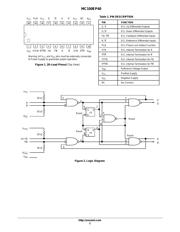
MARKING
DIAGRAM*
TSSOP−20
DT SUFFIX
CASE 948E
A = Assembly Location
L = Wafer Lot
Y = Year
W = Work Week
G = Pb−Free Package
20
1
http://onsemi.com
(Note: Microdot may be in either location)
100
EP40
ALYW G
1
20
G
See detailed ordering and shipping information in the package
dimensions section on page 7 of this data sheet.
ORDERING INFORMATION
*For additional marking information, refer to
Application Note AND8002/D.
Verzeichnis
- ・ Konfiguration des Pinbelegungsdiagramms on Seite 2
- ・ Abmessungen des Paketumrisses on Seite 8
- ・ Paket-Footprint-Pad-Layout on Seite 8
- ・ Teilenummerierungssystem on Seite 1 Seite 7 Seite 9
- ・ Markierungsinformationen on Seite 1 Seite 7 Seite 9
- ・ Typisches Anwendungsschaltbild on Seite 2
- ・ Technische Daten on Seite 7
- ・ Elektrische Spezifikation on Seite 5
- ・ Teilenummernliste on Seite 3