
herunterladen
© Semiconductor Components Industries, LLC, 2016
July, 2016 − Rev. 8
1 Publication Order Number:
MC10EL12/D
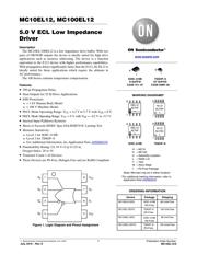
MC10EL12, MC100EL12
5.0 V ECL Low Impedance
Driver
Description
The MC10EL/100EL12 is a low impedance drive buffer. With two
pairs of OR/NOR outputs the device is ideally suited for high drive
applications such as memory addressing. The device is a function
equivalent to the E112 device with higher performance capabilities.
With propagation delays significantly faster than the E112, the EL12 is
ideally suited for those applications which require the ultimate in
AC performance.
The 100 Series contains temperature compensation.
Features
• 290 ps Propagation Delay
• Dual Outputs for 25 W Drive Applications
• ESD Protection:
♦ > 1 kV Human Body Model
♦ > 100 V Machine Model
• PECL Mode Operating Range: V
CC
= 4.2 V to 5.7 V with V
EE
= 0 V
• NECL Mode Operating Range: V
CC
= 0 V with V
EE
= −4.2 V to −5.7 V
• Internal Input Pulldown Resistors
• Meets or Exceeds JEDEC Spec EIA/JESD78 IC Latchup Test
• Moisture Sensitivity:
♦ Level 1 for SOIC−8 NB
♦ Level 3 for TSSOP−8
♦ For Additional Information, see Application Note AND8003/D
• Flammability Rating: UL 94 V−0 @ 0.125 in,
Oxygen Index: 28 to 34
• Transistor Count = 44 Devices
• These Devices are Pb-Free, Halogen Free and are RoHS Compliant
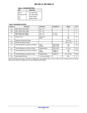
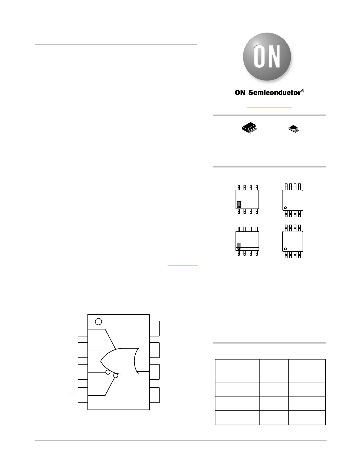
1
2
3
45
6
7
8
D
0
V
EE
V
CC
Figure 1. Logic Diagram and Pinout Assignment
Q
a
Q
b
D
1
Q
a
Q
b
HEL12
ALYW
G
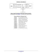
*For additional marking information, refer to
Application Note AND8002/D
.
MARKING DIAGRAMS*
KL12
ALYWG
G
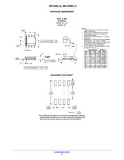
SOIC−8 NB
D SUFFIX
CASE 751−07
1
8
TSSOP−8
DT SUFFIX
CASE 948R−02
1
8
1
8
www.onsemi.com
KEL12
ALYW
G
1
8
HL12
ALYWG
G
1
8
1
8
(Note: Microdot may be in either location)
H = MC10
K = MC100
A = Assembly Location
L = Wafer Lot
Y = Year
W = Work Week
G = Pb-Free Package
SOIC−8 NB TSSOP−8
ORDERING INFORMATION
Device Package Shipping
MC10EL012DG SOIC−8 NB
(Pb-Free)
98 Units/Tube
MC10EL12DTG TSSOP−8
(Pb-Free)
100 Unit/Tube
MC100EL12DTG 100 Units/TubeTSSOP−8
(Pb-Free)
MC100EL12DG 98 Unit/Tube
SOIC−8 NB
(Pb-Free)
Verzeichnis
- ・ Konfiguration des Pinbelegungsdiagramms on Seite 2
- ・ Abmessungen des Paketumrisses on Seite 6 Seite 7
- ・ Paket-Footprint-Pad-Layout on Seite 6
- ・ Teilenummerierungssystem on Seite 1 Seite 7
- ・ Markierungsinformationen on Seite 1 Seite 5 Seite 7
- ・ Typisches Anwendungsschaltbild on Seite 1
- ・ Anwendungsbereich on Seite 1
- ・ Teilenummernliste on Seite 2