

herunterladen

Semiconductor Components Industries, LLC, 2003
November, 2003 − Rev. 1
1 Publication Order Number:
AND8090/D
AND8090/D
AC Characteristics of ECL
Devices
APPLICATION NOTE USAGE
This application note provides a general overview of the
AC characteristics that are specified on the
ON Semiconductor data sheets for MECL 10K, 10H,
100H, ECLinPS, ECLinPS Lite, and GigaComm SiGe
devices. Data sheet information takes precedence over this
application note if there are differences. This application
note includes the following information:
• AC Test Bench Information
• AC Characteristic Definitions
• AC Characteristic Test Methods
• AC Characteristic Examples
• AC Characteristic Symbols
• AC Characteristic References
TABLE OF CONTENTS
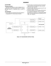
Lab Testing
Test Bench Overview 2. . . . . . . . . . . . . . . . . . . . . . . . . . .
Test Initialization 2. . . . . . . . . . . . . . . . . . . . . . . . . . . . . . .
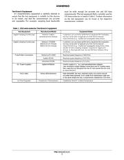
Test Bench Equipment 3. . . . . . . . . . . . . . . . . . . . . . . . . .
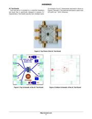
AC Test Boards 4. . . . . . . . . . . . . . . . . . . . . . . . . . . . . . . .
Signal Levels
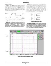
AC HIGH and LOW Levels 5. . . . . . . . . . . . . . . . . . . . . .
Oscilloscope Averaging 5. . . . . . . . . . . . . . . . . . . . . . . . .
Input Levels 5. . . . . . . . . . . . . . . . . . . . . . . . . . . . . . . . . . .
Output Levels 5. . . . . . . . . . . . . . . . . . . . . . . . . . . . . . . . .
Output Swing 6. . . . . . . . . . . . . . . . . . . . . . . . . . . . . . . . . .
Signal Timing
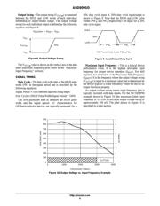
Duty Cycle 6. . . . . . . . . . . . . . . . . . . . . . . . . . . . . . . . . . . .
Maximum Input Frequency 6. . . . . . . . . . . . . . . . . . . . . .
Differential Characteristics
Differential Input Application 7. . . . . . . . . . . . . . . . . . . . .
Unused Output Termination 7. . . . . . . . . . . . . . . . . . . . . .
Differential Crosspoint 7. . . . . . . . . . . . . . . . . . . . . . . . . .
Input Voltage Swing 7. . . . . . . . . . . . . . . . . . . . . . . . . . . .
Test Input Swing 7. . . . . . . . . . . . . . . . . . . . . . . . . . . . . . .
Differential Characteristics (continued)
Common Mode Range 7. . . . . . . . . . . . . . . . . . . . . . . . . .
Differential Input Example 8. . . . . . . . . . . . . . . . . . . . . . .
Single−Ended Characteristics
Single−Ended Inputs 8. . . . . . . . . . . . . . . . . . . . . . . . . . .
Single−Ended 50% Points 8. . . . . . . . . . . . . . . . . . . . . . .
Single–Ended Input Voltage Range 8. . . . . . . . . . . . . . .
Single–Ended Input Test Level 8. . . . . . . . . . . . . . . . . . .
Differential Inputs (Single–Ended Mode) 9. . . . . . . . . . .
Timing Characteristics
Output Rise and Fall Times 9. . . . . . . . . . . . . . . . . . . . . .
Propagation Delay 10. . . . . . . . . . . . . . . . . . . . . . . . . . . .
Skew (Duty Cycle) 11. . . . . . . . . . . . . . . . . . . . . . . . . . . .
Skew (Within Device) 11. . . . . . . . . . . . . . . . . . . . . . . . . .
Skew (Device to Device) 11. . . . . . . . . . . . . . . . . . . . . . .
Minimum Input Pulse Width 11. . . . . . . . . . . . . . . . . . . . .
Setup and Hold Time 12. . . . . . . . . . . . . . . . . . . . . . . . . .
Set and Reset Recovery Time 14. . . . . . . . . . . . . . . . . .
Jitter
Jitter Overview 15. . . . . . . . . . . . . . . . . . . . . . . . . . . . . . . .
Random Jitter 15. . . . . . . . . . . . . . . . . . . . . . . . . . . . . . . .
RJ Confidence Levels 15. . . . . . . . . . . . . . . . . . . . . . . . .
Total RJ Test Setup 16. . . . . . . . . . . . . . . . . . . . . . . . . . . .
Test Equipment RJ Test Setup 16. . . . . . . . . . . . . . . . . .
DUT RJ Calculation 16. . . . . . . . . . . . . . . . . . . . . . . . . . .
Deterministic Jitter 17. . . . . . . . . . . . . . . . . . . . . . . . . . . .
Total DJ Test Setup 17. . . . . . . . . . . . . . . . . . . . . . . . . . . .
Test Equipment DJ Test Setup 18. . . . . . . . . . . . . . . . . .
DUT DJ Calculation 18. . . . . . . . . . . . . . . . . . . . . . . . . . .
Symbols and Acronyms
Symbols and Acronyms Table 19. . . . . . . . . . . . . . . . . . .
References
AC Characteristic References 20. . . . . . . . . . . . . . . . . . .
APPLICATION NOTE
http://onsemi.com
Verzeichnis
- ・ Teilenummerierungssystem on Seite 20
- ・ Blockdiagramm on Seite 4