
herunterladen
© Semiconductor Components Industries, LLC, 2016
July, 2016 − Rev. 11
1 Publication Order Number:
MC100LVEL39/D
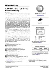
MC100LVEL39
3.3V ECL ÷2/4, ÷4/6 Clock
Generation Chip
Description
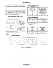
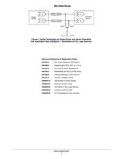
The MC100LVEL39 is a low skew ÷2/4, ÷4/6 clock generation chip
designed explicitly for low skew clock generation applications. The
internal dividers are synchronous to each other, therefore, the common
output edges are all precisely aligned. The device can be driven by
either a differential or single-ended input signal. In addition, by using
the V
BB
output, a sinusoidal source can be AC coupled into the device.
The common enable (EN
) is synchronous so that the internal dividers
will only be enabled/disabled when the internal clock is already in the
LOW state. This avoids any chance of generating a runt clock pulse on
the internal clock when the device is enabled/disabled as can happen with
an asynchronous control. An internal runt pulse could lead to losing
synchronization between the internal divider stages. The internal enable
flip-flop is clocked on the falling edge of the input clock, therefore, all
associated specification limits are referenced to the negative edge of the
clock input.
Upon startup, the internal flip-flops will attain a random state;
therefore, for systems which utilize multiple LVEL39s, the Master Reset
(MR) input must be asserted to ensure synchronization. For systems
which only use one LVEL39, the MR pin need not be exercised as the
internal divider design ensures synchronization between the ÷2/4 and the
÷4/6 outputs of a single device.
The V
BB
pin, an internally generated voltage supply, is available to this
device only. For single-ended input conditions, the unused differential
input is connected to V
BB
as a switching reference voltage. V
BB
may also
rebias AC coupled inputs. When used, decouple V
BB
and V
CC
via
a.01 mF capacitor and limit current sourcing or sinking to 0.5 mA. When
not used, V
BB
should be left open.
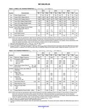
Features
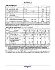
• 50 ps Maximum Output-to-Output Skew
• Synchronous Enable/Disable
• Master Reset for Synchronization
• ESD Protection: Human Body Model; > 2 kV
• The 100 Series Contains Temperature Compensation
• PECL Mode Operating Range:
V
CC
= 3.0 V to 3.8 V with V
EE
= 0 V
• NECL Mode Operating Range:
V
CC
= 0 V with V
EE
= −3.0 V to −3.8 V
• Internal Input Pulldown Resistors
• Meets or Exceeds JEDEC Spec EIA/JESD78 IC Latchup Test
• Moisture Sensitivity: Level 3 (Pb-Free)
♦ For Additional Information, see Application Note
AND8003/D
• Flammability Rating: UL 94 V−0 @ 0.125 in,
Oxygen Index: 28 to 34
• Transistor Count = 419 devices
• These Devices are Pb-Free, Halogen Free and are
RoHS Compliant
A = Assembly Location
WL = Wafer Lot
YY = Year
WW = Work Week
G = Pb-Free Package
*For additional marking information, refer to
Application Note AND8002/D
.
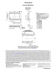
MARKING DIAGRAM*
SOIC−20 WB
DW SUFFIX
CASE 751D
20
1
100LVEL39
AWLYYWWG
www.onsemi.com
ORDERING INFORMATION
Device Package Shipping
†
MC100LVEL39DWR2G SOIC−20 WB
(Pb-Free)
1000/Tape & Reel
†For information on tape and reel specifications, in-
cluding part orientation and tape sizes, please refer
to our Tape and Reel Packaging Specifications
Brochure, BRD8011/D
.
Verzeichnis
- ・ Konfiguration des Pinbelegungsdiagramms on Seite 2
- ・ Abmessungen des Paketumrisses on Seite 6
- ・ Paket-Footprint-Pad-Layout on Seite 6
- ・ Teilenummerierungssystem on Seite 1 Seite 6
- ・ Markierungsinformationen on Seite 1 Seite 5 Seite 6
- ・ Typisches Anwendungsschaltbild on Seite 2
- ・ Beschreibung der Funktionen on Seite 1 Seite 2
- ・ Technische Daten on Seite 1
- ・ Teilenummernliste on Seite 3