

herunterladen
© Semiconductor Components Industries, LLC, 2014
July, 2014 − Rev. 8
1 Publication Order Number:
MC14008B/D
MC14008B
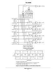
4-Bit Full Adder
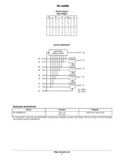
The MC14008B 4−bit full adder is constructed with MOS
P−Channel and N−Channel enhancement mode devices in a single
monolithic structure. This device consists of four full adders with fast
internal look−ahead carry output. It is useful in binary addition and
other arithmetic applications. The fast parallel carry output bit allows
high−speed operation when used with other adders in a system.
Features
• Look−Ahead Carry Output
• Diode Protection on All Inputs
• All Outputs Buffered
• Supply Voltage Range = 3.0 Vdc to 18 Vdc
• Capable of Driving Two Low−Power TTL Loads or One
Low−Power Schottky TTL Load Over the Rated Temperature Range
• Pin−for−Pin Replacement for CD4008B
• This Device is Pb−Free and is RoHS Compliant
MAXIMUM RATINGS (Voltages Referenced to V
SS
)
Symbol
Parameter Value Unit
V
DD
DC Supply Voltage Range −0.5 to +18.0 V
V
in
, V
out
Input or Output Voltage Range
(DC or Transient)
−0.5 to V
DD
+ 0.5 V
I
in
, I
out
Input or Output Current
(DC or Transient) per Pin
±10 mA
P
D
Power Dissipation, per Package
(Note 1)
500 mW
T
A
Ambient Temperature Range −55 to +125 °C
T
stg
Storage Temperature Range −65 to +150 °C
T
L
Lead Temperature
(8−Second Soldering)
260 °C
Stresses exceeding Maximum Ratings may damage the device. Maximum
Ratings are stress ratings only. Functional operation above the Recommended
Operating Conditions is not implied. Extended exposure to stresses above the
Recommended Operating Conditions may affect device reliability.
1. Temperature Derating: “D/DW” Package: –7.0 mW/_C From 65_C To 125_C
This device contains protection circuitry to guard against damage due to high
static voltages or electric fields. However, precautions must be taken to avoid
applications of any voltage higher than maximum rated voltages to this
high−impedance circuit. For proper operation, V
in
and V
out
should be constrained
to the range V
SS
≤ (V
in
or V
out
) ≤ V
DD
.
Unused inputs must always be tied to an appropriate logic voltage level
(e.g., either V
SS
or V
DD
). Unused outputs must be left open.
http://onsemi.com
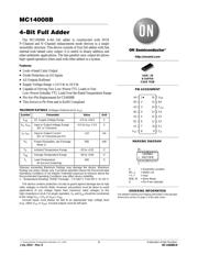
MARKING DIAGRAM
SOIC−16
D SUFFIX
CASE 751B
14008BG
AWLYWW
A = Assembly Location
WL, L = Wafer Lot
YY, Y = Year
WW, W = Work Week
G = Pb−Free Indicator
See detailed ordering and shipping information in the package
dimensions section on page 2 of this data sheet.
ORDERING INFORMATION
1
16
13
14
15
16
9
10
11
125
4
3
2
1
8
7
6
S3
S4
C
out
B4
V
DD
C
in
S1
S2
B2
A3
B3
A4
V
SS
A1
B1
A2
PIN ASSIGNMENT
Verzeichnis
- ・ Konfiguration des Pinbelegungsdiagramms on Seite 1
- ・ Abmessungen des Paketumrisses on Seite 7
- ・ Paket-Footprint-Pad-Layout on Seite 7
- ・ Teilenummerierungssystem on Seite 1 Seite 2 Seite 7
- ・ Markierungsinformationen on Seite 1 Seite 7
- ・ Blockdiagramm on Seite 2
- ・ Typisches Anwendungsschaltbild on Seite 6
- ・ Technische Daten on Seite 2
- ・ Elektrische Spezifikation on Seite 3