
herunterladen
© Semiconductor Components Industries, LLC, 2013
May, 2013 − Rev. 9
1 Publication Order Number:
MC14503B/D
MC14503B
Hex Non-Inverting 3-State
Buffer
The MC14503B is a hex non−inverting buffer with 3−state outputs,
and a high current source and sink capability. The 3−state outputs
make it useful in common bussing applications. Two disable controls
are provided. A high level on the Disable A input causes the outputs of
buffers 1 through 4 to go into a high impedance state and a high level
on the Disable B input causes the outputs of buffers 5 and 6 to go into a
high impedance state.
Features
• 3−State Outputs
• TTL Compatible — Will Drive One TTL Load Over Full
Temperature Range
• Supply Voltage Range = 3.0 Vdc to 18 Vdc
• Two Disable Controls for Added Versatility
• Pin for Pin Replacement for MM80C97 and 340097
• These Devices are Pb−Free and are RoHS Compliant
• NLV Prefix for Automotive and Other Applications Requiring
Unique Site and Control Change Requirements; AEC−Q100
Qualified and PPAP Capable
MAXIMUM RATINGS (Voltages Referenced to V
SS
) (Note 1)
Parameter
Symbol Value Unit
DC Supply Voltage Range V
DD
−0.5 to +18.0 V
Input or Output Voltage Range
(DC or Transient)
V
in
, V
out
−0.5 to V
DD
+ 0.5
V
Input Current (DC or Transient) per Pin I
in
± 10 mA
Output Current (DC or Transient) per Pin I
out
± 25 mA
Power Dissipation, per Package (Note 2) P
D
500 mW
Ambient Temperature Range T
A
−55 to +125 °C
Storage Temperature Range −65 to +150 °C
Lead Temperature (8−Second Soldering) 260 °C
Stresses exceeding Maximum Ratings may damage the device. Maximum
Ratings are stress ratings only. Functional operation above the Recommended
Operating Conditions is not implied. Extended exposure to stresses above the
Recommended Operating Conditions may affect device reliability.
1. Maximum Ratings are those values beyond which damage to the device may
occur.
2. Temperature Derating:
Plastic “P and D/DW” Packages: – 7.0 mW/_C From 65_C To 125_C
This device contains protection circuitry to guard against damage due to high
static voltages or electric fields. However, precautions must be taken to avoid
applications of any voltage higher than maximum rated voltages to this
high−impedance circuit. For proper operation, V
in
and V
out
should be constrained
to the range V
SS
v (V
in
or V
out
) v V
DD
.
Unused inputs must always be tied to an appropriate logic voltage level
(e.g., either V
SS
or V
DD
). Unused outputs must be left open.
A = Assembly Location
WL, L = Wafer Lot
YY, Y = Year
WW, W = Work Week
G = Pb−Free Package
MARKING
DIAGRAMS
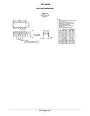
PDIP−16
P SUFFIX
CASE 648
SOIC−16
D SUFFIX
CASE 751B
1
16
14503BG
AWLYWW
See detailed ordering and shipping information in the package
dimensions section on page 2 of this data sheet.
ORDERING INFORMATION
16
1
MC14503BCP
AWLYYWWG
http://onsemi.com
1
1
Verzeichnis
- ・ Konfiguration des Pinbelegungsdiagramms on Seite 2
- ・ Abmessungen des Paketumrisses on Seite 6 Seite 7
- ・ Paket-Footprint-Pad-Layout on Seite 7
- ・ Teilenummerierungssystem on Seite 1 Seite 2 Seite 7
- ・ Markierungsinformationen on Seite 1 Seite 7
- ・ Typisches Anwendungsschaltbild on Seite 2
- ・ Technische Daten on Seite 2
- ・ Anwendungsbereich on Seite 1 Seite 2
- ・ Elektrische Spezifikation on Seite 3