
herunterladen
Semiconductor Components Industries, LLC, 2003
December, 2003 − Rev. 12
1 Publication Order Number:
MC74VHC1G09/D
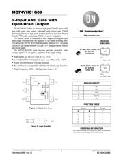
MC74VHC1G09
2−Input AND Gate with
Open Drain Output
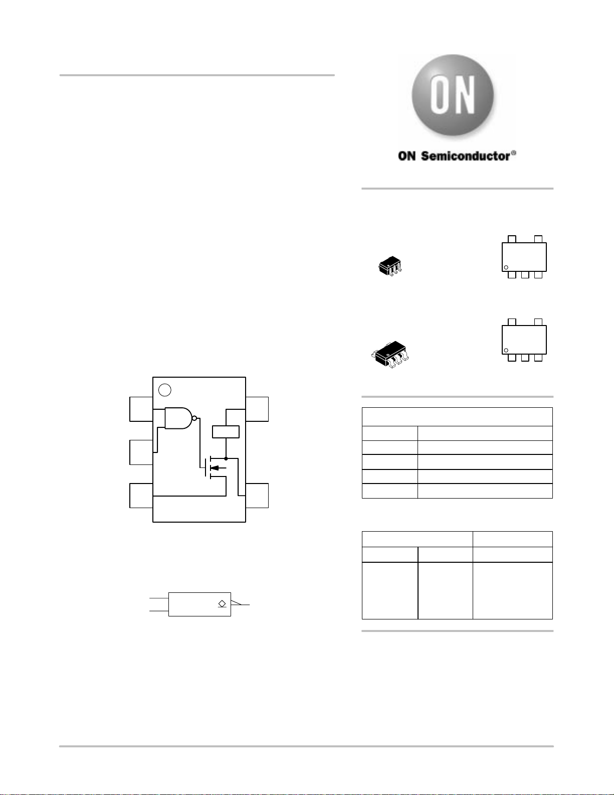
The MC74VHC1G09 is an advanced high speed CMOS 2−input AND
gate with open drain output fabricated with silicon gate CMOS
technology. It achieves high speed operation similar to equivalent Bipolar
Schottky TTL while maintaining CMOS low power dissipation.
The internal circuit is composed of three stages, including an open
drain output which provides the capability to set output switching level.
This allows the MC74VHC1G09 to be used to interface 5.0 V circuits to
circuits of any voltage between V
CC
and 7.0 V using an external resistor
and power supply.
The MC74VHC1G09 input structure provides protection when
voltages up to 7.0 V are applied, regardless of the supply voltage.
• High Speed: t
PD
= 4.3 ns (Typ) at V
CC
= 5.0 V
• Low Internal Power Dissipation: I
CC
= 1 A (Max) at T
A
= 25°C
• Power Down Protection Provided on Inputs
• Pin and Function Compatible with Other Standard Logic Families
• Chip Complexity: FETs = 62; Equivalent Gates = 16
V
CC
IN B
IN A
OUT Y
GND
IN A
IN B
OUT Y
&
OVT
Figure 1. Pinout (Top View)
Figure 2. Logic Symbol
1
2
3
4
5
L
L
H
H
L
H
L
H
FUNCTION TABLE
Inputs Output
AB
L
L
L
Z
Y
See detailed ordering and shipping information in the package
dimensions section on page 4 of this data sheet.
ORDERING INFORMATION
MARKING
DIAGRAMS
SC−88A / SOT−353/SC−70
DF SUFFIX
CASE 419A
Pin 1
d = Date Code
VX
d
TSOP−5/SOT−23/SC−59
DT SUFFIX
CASE 483
Pin 1
d = Date Code
VX
d
PIN ASSIGNMENT
1
2
3 GND
IN B
IN A
4
5V
CC
OUT Y
http://onsemi.com
Verzeichnis
- ・ Konfiguration des Pinbelegungsdiagramms on Seite 1
- ・ Abmessungen des Paketumrisses on Seite 7 Seite 8
- ・ Paket-Footprint-Pad-Layout on Seite 7 Seite 8
- ・ Teilenummerierungssystem on Seite 1 Seite 4 Seite 8
- ・ Markierungsinformationen on Seite 1
- ・ Label-Indikator on Seite 6
- ・ Technische Daten on Seite 4
- ・ Elektrische Spezifikation on Seite 3