


herunterladen

© 2005 Microchip Technology Inc. DS00980A-page 1
AN980
INTRODUCTION
Today’s electronic circuits require a number of different
voltage potentials. Powering silicon devices like
microcontrollers or digital logic require a different volt-
age than bias supplies or powering strings of LEDs. A
system can very easily contain a combination of circuits
that require different voltages. With only a single input
voltage delivered to the system, a power regulator is
needed to produce the necessary voltages.
The power regulator can be an inductor-based, switch-
mode power converter, a switched capacitor charge
pump or a linear regulator. Each regulator has it’s own
advantages and disadvantages, but it is the particular
application requirements that determine which type of
power regulator is best suited.
This application note focuses on inductor-based,
switchmode power converters, more specifically – the
boost regulator topology. The boost is one of the funda-
mental switchmode power topologies. The other being
the buck regulator. From these two topologies, all other
switchmode power supply topologies are derived. The
buck topology is used to provide a regulated voltage
that is lower than the unregulated input voltage source.
The boost topology produces a regulated output volt-
age that is higher than the unregulated input voltage
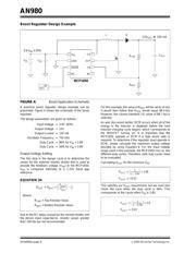
source. An example of a boost regulator design will be
explored using Microchip’s MCP1650 boost controller.
UNDERSTANDING THE BOOST
TOPOLOGY
Before we begin the design example, it is important to
understand how the boost converter produces an
output voltage that is always greater than the input
voltage. In order to do this, we must analyze the boost
circuits in Figure 1. During one switching cycle, the
switch (S1) transitions between a closed and opened
position. If the switching cycle begins with S1 in the
closed position (as in Figure 1B), diode D
1
is reverse-
biased, the voltage across the boost inductor (L
1
) is
equal to V
IN
and the current is ramping up in L
1
. Any
load requirements during this phase are supplied by
the output capacitor (C
1
). When S1 switches to the
open position, as in Figure 1C, D
1
is forward-biased,
the voltage across L
1
is V
IN
minus V
OUT
and energy is
transferred from L
1
(as well as the input source) to the
load. The energy depleted from C
1
is also replaced.
The output voltage is greater than the input because
both the input source and L
1
supply energy to the load
during this phase. A practical realization of the boost
converter is illustrated in Figure 1D, where S1 is
replaced by a N-channel MOSFET. A graphical
representation of the boost waveforms can be found in
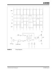
Figure 2.
Author: Cliff Ellison
Microchip Technology Inc.
Designing a Boost-Switching Regulator with the MCP1650