

herunterladen
2016 Microchip Technology Inc. DS00002089A-page 1
AN2089
INTRODUCTION
This package application note provides the guidelines
for the handling and assembly of Microchip QFN and
DFN packages during the Printed Circuit Board (PCB)
assembly. In addition, it provides general information
for the PCB land pattern design and component rework
guidelines.
SCOPE
This application note contains generic information for
various Microchip QFN and DFN packages assembled
internally or at external subcontractors. Specific infor-
mation about each device is not provided. To develop a
specific solution, actual experience and development
efforts are required to optimize the assembly process
and application design per individual device require-
ments, industry standards (such as IPC and JEDEC),
and prevalent practices in the assembly environment.
For more details about the specific devices contained
in this note, visit www.microchip.com or contact your
local Microchip sales office.
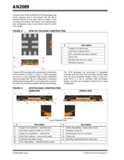
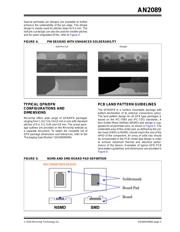
PACKAGE DESCRIPTION AND
CONSTRUCTION
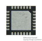
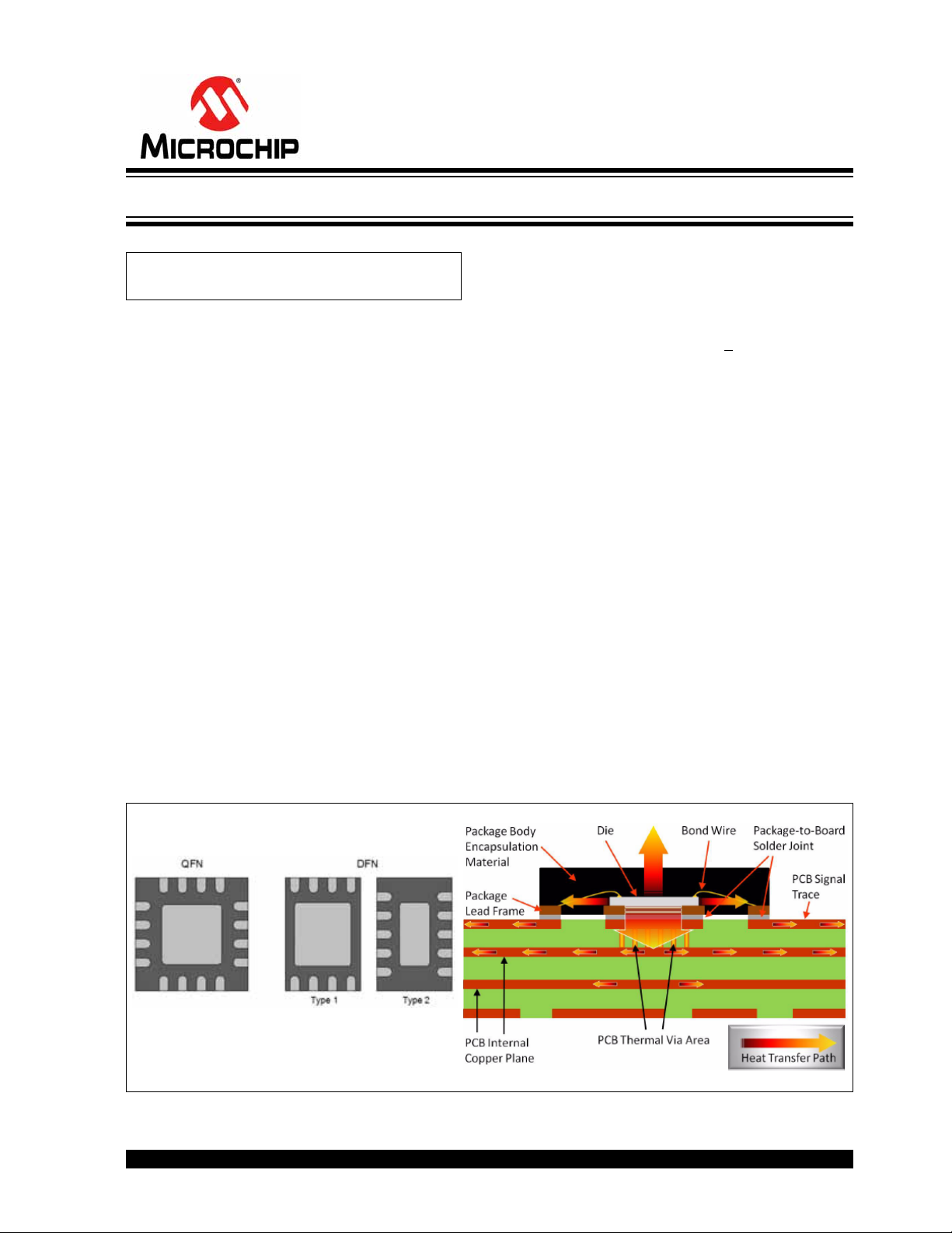
QFN and DFN packages are plastic encapsulated lead-
frame-based packages, which are near Chip Scale
Package (CSP) with a low profile (<
1.0 mm). This pack-
age type uses perimeter lands/pins on the bottom of
the package to provide electrical contacts to the PCB.
Perimeter pins can be arranged in dual-in-line (DFN) or
quad (QFN) configuration. Pins in DFN packages,
when rectangular, can be arranged on the short side
(Type 1), or on the long side (Type 2), see Figure 1. The
package also has an exposed center pad (ePAD) as a
thermal enhancement at the bottom of the package.
The ePAD needs to be soldered directly to the PCB for
an efficient thermal path from the die to the board (see
Figure 1). The center pad also enables stable ground
through use of down-bonds and electrical connections
through conductive die attach material. The QFN and
DFN packages are offered in various pincounts and
body sizes, and have the following features:
• Small overall dimensions, compared to leaded
packages, which helps maximize board space
• Thermally enhanced plastic package
• Very high design flexibility due to the etching
process of the leadframe
• Easy accommodation of multi die assemblies,
where separated pads are required
• Standard SMT performance characteristics
FIGURE 1: QFN/DFN LEADS/PINS CONFIGURATION AND HEAT TRANSFER
Authors: Simeon Iliev
Microchip Technology Inc.
Package Application Note for QFN and DFN Packages