

herunterladen
© Semiconductor Components Industries, LLC, 2013
September, 2013 − Rev. 5
1 Publication Order Number:
MJW21193/D
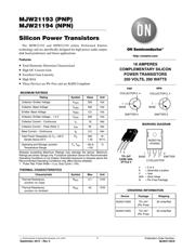
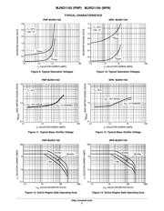
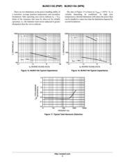
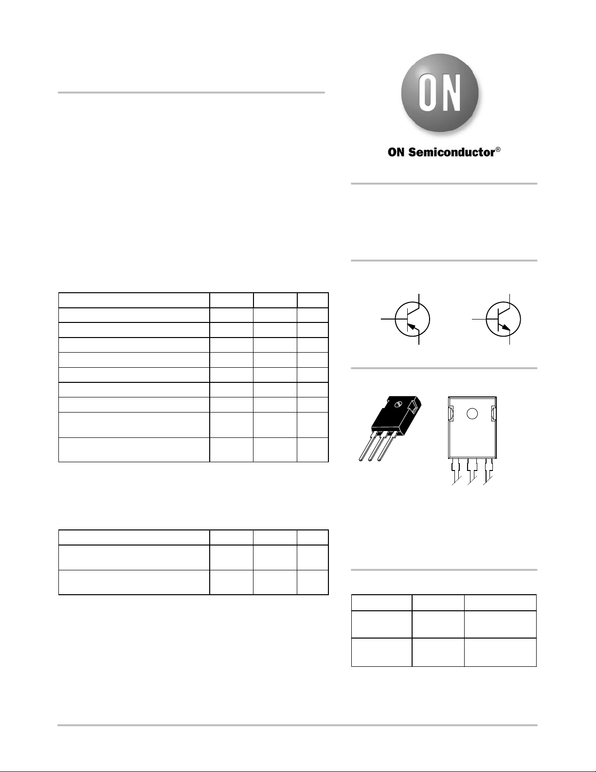
MJW21193 (PNP)
MJW21194 (NPN)
Silicon Power Transistors
The MJW21193 and MJW21194 utilize Perforated Emitter
technology and are specifically designed for high power audio output,
disk head positioners and linear applications.
Features
• Total Harmonic Distortion Characterized
• High DC Current Gain
• Excellent Gain Linearity
• High SOA
• These Devices are Pb−Free and are RoHS Compliant
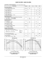
MAXIMUM RATINGS
Rating Symbol Value Unit
Collector−Emitter Voltage V
CEO
250 Vdc
Collector−Base Voltage V
CBO
400 Vdc
Emitter−Base Voltage V
EBO
5.0 Vdc
Collector−Emitter Voltage − 1.5 V V
CEX
400 Vdc
Collector Current − Continuous I
C
16 Adc
Collector Current − Peak (Note 1) I
CM
30 Adc
Base Current − Continuous I
B
5.0 Adc
Total Power Dissipation @ T
C
= 25°C
Derate Above 25°C
P
D
200
1.43
W
W/°C
Operating and Storage Junction
Temperature Range
T
J
, T
stg
− 65 to
+150
°C
Stresses exceeding Maximum Ratings may damage the device. Maximum
Ratings are stress ratings only. Functional operation above the Recommended
Operating Conditions is not implied. Extended exposure to stresses above the
Recommended Operating Conditions may affect device reliability.
1. Pulse Test: Pulse Width = 5 ms, Duty Cycle ≤ 10%.
THERMAL CHARACTERISTICS
Characteristic Symbol Max Unit
Thermal Resistance,
Junction−to−Case
R
θ
JC
0.7 °C/W
Thermal Resistance,
Junction−to−Ambient
R
θ
JA
40 °C/W
16 AMPERES
COMPLEMENTARY SILICON
POWER TRANSISTORS
250 VOLTS, 200 WATTS
Device Package Shipping
ORDERING INFORMATION
MARKING DIAGRAM
x = 3 or 4
A = Assembly Location
Y = Year
WW = Work Week
G = Pb−Free Package
MJW21193G TO−247
(Pb−Free)
30 Units/Rail
MJW21194G TO−247
(Pb−Free)
30 Units/Rail
http://onsemi.com
TO−247
CASE 340L
STYLE 3
1
2
3
MJW2119x
AYWWG
1
BASE
2 COLLECTOR
3
EMITTER
1
BASE
EMITTER 3
COLLECTOR 2, 4
1
BASE
EMITTER 3
COLLECTOR 2, 4
PNP
NPN
Verzeichnis