
herunterladen
Semiconductor Components Industries, LLC, 2012
January, 2012 − Rev. 19
1 Publication Order Number:
MM3Z2V4ST1/D
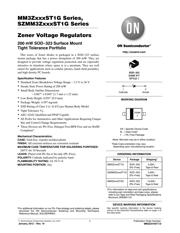
MM3ZxxxST1G Series,
SZMM3ZxxxST1G Series
Zener Voltage Regulators
200 mW SOD−323 Surface Mount
Tight Tolerance Portfolio
This series of Zener diodes is packaged in a SOD−323 surface
mount package that has a power dissipation of 200 mW. They are
designed to provide voltage regulation protection and are especially
attractive in situations where space is at a premium. They are well
suited for applications such as cellular phones, hand−held portables,
and high density PC boards.
Specification Features
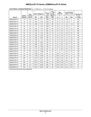
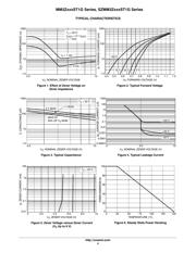
Standard Zener Breakdown Voltage Range − 3.3 V to 36 V
Steady State Power Rating of 200 mW
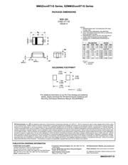
Small Body Outline Dimensions:
− 0.067 x 0.049 (1.7 mm x 1.25 mm)
Low Body Height: 0.035 (0.9 mm)
Package Weight: 4.507 mg/unit
ESD Rating of Class 3 (> 16 kV) per Human Body Model
Tight Tolerance V
Z
AEC−Q101 Qualified and PPAP Capable
SZ Prefix for Automotive and Other Applications Requiring Unique
Site and Control Change Requirements
These Devices are Pb−Free, Halogen Free/BFR Free and are RoHS
Compliant*
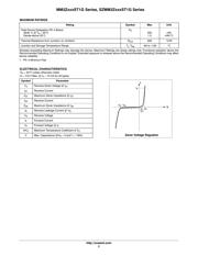
Mechanical Characteristics:
CASE:
Void-free, transfer-molded plastic
FINISH: All external surfaces are corrosion resistant
MAXIMUM CASE TEMPERATURE FOR SOLDERING PURPOSES:
260C for 10 Seconds
LEADS: Plated with Pb−Sn or Sn only (Pb−Free)
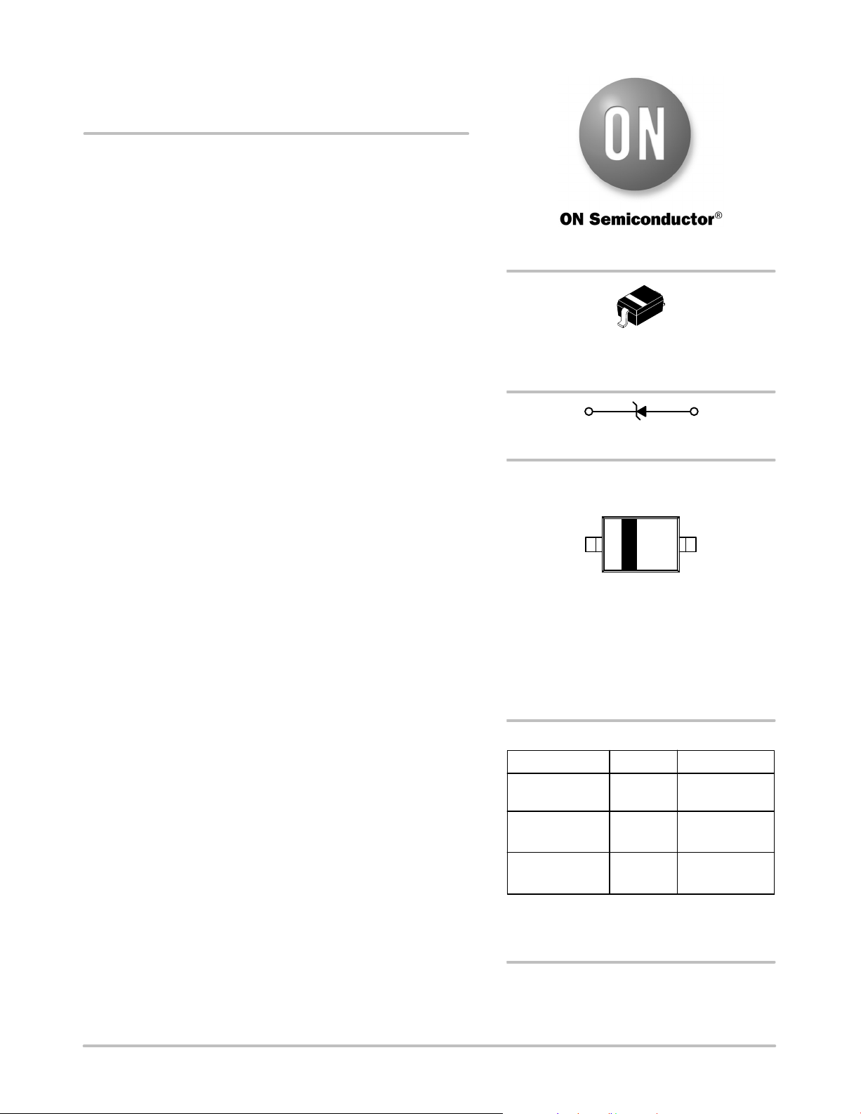
POLARITY: Cathode indicated by polarity band
FLAMMABILITY RATING: UL 94 V−0
MOUNTING POSITION: Any
*For additional information on our Pb−Free strategy and soldering details, please
download the ON Semiconductor Soldering and Mounting Techniques
Reference Manual, SOLDERRM/D.
Device Package Shipping
†
ORDERING INFORMATION
SOD−323
CASE 477
STYLE 1
1
Cathode
2
Anode
MARKING DIAGRAM
See specific marking information in the device marking
column of the Electrical Characteristics table on page 3 of
this data sheet.
DEVICE MARKING INFORMATION
XX = Specific Device Code
M = Date Code*
G = Pb−Free Package
†For information on tape and reel specifications,
including part orientation and tape sizes, please
refer to our Tape and Reel Packaging Specifications
Brochure, BRD8011/D.
http://onsemi.com
MM3ZxxxST1G SOD−323
(Pb−Free)
3,000 /
Tape & Reel
MM3ZxxxST3G SOD−323
(Pb−Free)
10,000 /
Tape & Reel
XXMG
G
*Date Code orientation may vary
depending upon manufacturing location.
(Note: Microdot may be in either location)
SZMM3ZxxxST1G SOD−323
(Pb−Free)
3,000 /
Tape & Reel
Verzeichnis