


herunterladen
Semiconductor Components Industries, LLC, 2011
November, 2011 − Rev. 6
1 Publication Order Number:
MMBT589LT1/D
MMBT589LT1G,
NSVMMBT589LT1G
High Current Surface Mount
PNP Silicon Switching
Transistor for Load
Management in
Portable Applications
Features
AEC−Q101 Qualified and PPAP Capable
NSV Prefix for Automotive and Other Applications Requiring
Unique Site and Control Change Requirements
These Devices are Pb−Free, Halogen Free/BFR Free and are RoHS
Compliant*
MAXIMUM RATINGS (T
A
= 25C)
Rating
Symbol Value Unit
Collector−Emitter Voltage V
CEO
−30 Vdc
Collector−Base Voltage V
CBO
−50 Vdc
Emitter−Base Voltage V
EBO
−5.0 Vdc
Collector Current − Continuous I
C
−1.0 Adc
Collector Current − Peak I
CM
−2.0 A
THERMAL CHARACTERISTICS
Characteristic Symbol Max Unit
Total Device Dissipation FR−5 Board,
(Note 1) T
A
= 25C
Derate above 25C
P
D
310
2.5
mW
mW/C
Thermal Resistance
Junction−to−Ambient (Note 1)
R
q
JA
403
C/W
Total Device Dissipation Alumina
Substrate, (Note 2) T
A
= 25C
Derate above 25C
P
D
710
5.7
mW
mW/C
Thermal Resistance
Junction−to−Ambient (Note 2)
R
q
JA
176
C/W
Total Device Dissipation (Ref. Figure 8)
(Single Pulse < 10 sec.)
P
Dsingle
575 mW
Junction and Storage Temperature T
J
, T
stg
−55 to +150 C
Stresses exceeding Maximum Ratings may damage the device. Maximum
Ratings are stress ratings only. Functional operation above the Recommended
Operating Conditions is not implied. Extended exposure to stresses above the
Recommended Operating Conditions may affect device reliability.
1. FR−4 @ Minimum Pad
2. FR−4 @ 1.0 X 1.0 inch Pad
*For additional information on our Pb−Free strategy and soldering details, please
download the ON Semiconductor Soldering and Mounting Techniques
Reference Manual, SOLDERRM/D.
http://onsemi.com
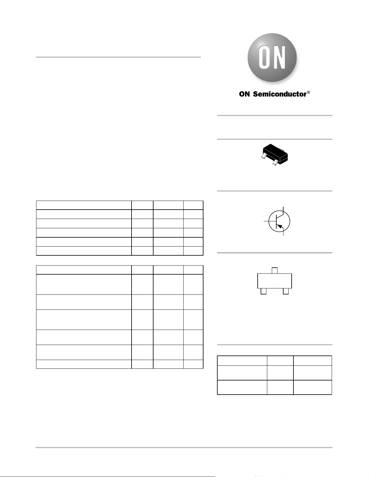
SOT−23 (TO−236)
CASE 318
STYLE 6
Device Package Shipping
†
ORDERING INFORMATION
†For information on tape and reel specifications,
including part orientation and tape sizes, please
refer to our Tape and Reel Packaging Specifications
Brochure, BRD8011/D.
MMBT589LT1G SOT−23
(Pb−Free)
3,000 /
Tape & Reel
*Date Code orientation and/or overbar may
vary depending upon manufacturing location.
1
G3 M G
G
G3 = Device Code
M = Date Code*
G = Pb−Free Package
(Note: Microdot may be in either location)
MARKING DIAGRAM
30 VOLTS, 2.0 AMPS
PNP TRANSISTORS
COLLECTOR
3
1
BASE
2
EMITTER
NSVMMBT589LT1G SOT−23
(Pb−Free)
3,000 /
Tape & Reel
Verzeichnis