


herunterladen
MRF1K50N MRF1K50GN
1
RF Device Data
NXP Semiconductors
RF Power LDMOS Transistors
High Ruggedness N--Channel
Enhancement--Mode Lateral MOSFETs
These high ruggedness devices are designed for use in high VSWR industrial,
scientific and medical applications, as well as radio and VH F TV broadcast,
sub--GHz aerospace and mobile radio applications. Their unmatched input and
output design allows for wide frequency range use from 1.8 to 500 MHz.
Typical Performance: V
DD
=50Vdc
Frequency
(MHz)
Signal Type
P
out
(W)
G
ps
(dB)
η
D
(%)
87.5--108
(1,2)
CW 1421 CW 23.1 83.2
230
(3,4)
Pulse
(100 μsec, 20% Duty Cycle)
1500 Peak 23.4 75.1
Load Mismatch/Ruggedness
Frequency
(MHz)
Signal Type VSWR
P
in
(W)
Test
Voltage
Result
230
(3)
Pulse
(100 μsec, 20%
Duty Cycle)
> 65:1 at all
Phase Angles
15 Peak
(3 dB
Overdrive)
50 No Device
Degradation
1. Data from 87.5–108 MHz broadband reference circuit (page 5).
2. The values shown are the center band performance numbers across the indicated
frequency range.
3. Data from 230 MHz narrowband production test fixture (page 11).
4. All data measured in fixture with device soldered to heatsink.
Features
• High drain--source avalanche energy absorption capability
• Unmatched input and output allowing wide frequency range utilization
• Device can be used single--ended or in a push--pull configuration
• Characterizedfrom30to50Vforeaseofuse
• Suitable for linear application
• Integrated ESD protection with greater negative gate--source voltage range
for improved Class C operation
• Recommended driver: MRFE6VS25N (25 W)
Typical Applications
• Industrial, Scientific, Medical (ISM)
– Laser generation
– Plasma etching
– Particle accelerators
– MRI and other medical applications
– Industrial heating, welding and drying systems
• Broadcast
– Radio broadcast
– VHF TV broadcast
• Aerospace
– VHF omnidirectional range (VOR)
– HF and VHF communications
– Weather radar
• Mobile Radio
– VHF and UHF base stations
Document Number: MRF1K50N
Rev. 0, 1 1/2016
NXP Semiconductors
Technical Data
1.8–500 MHz, 1500 W CW, 50 V
WIDEBAND
RF POWER LDMOS TRANSISTORS
MRF1K50N
MRF1K50GN
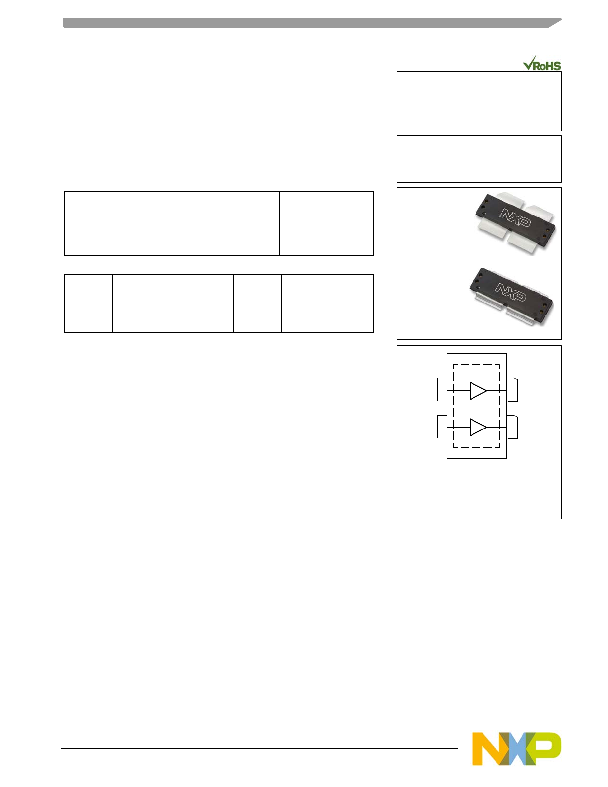
(Top View)
Figure 1. Pin Connections
Note: Exposed backside of the package is
the source terminal for the transistor.
Drain A
31
42
Drain B
Gate A
Gate B
OM--1230--4L
PLASTIC
MRF1K50N
OM--1230G--4L
PLASTIC
MRF1K50GN
© 2016 NXP B.V.
Verzeichnis