
herunterladen
Semiconductor Components Industries, LLC, 2000
November, 2000 – Rev. 3
1 Publication Order Number:
MTD3055VL/D
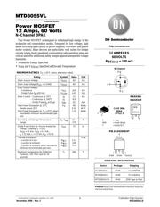
MTD3055VL
Preferred Device
Power MOSFET
12 Amps, 60 Volts
N–Channel DPAK
This Power MOSFET is designed to withstand high energy in the
avalanche and commutation modes. Designed for low voltage, high
speed switching applications in power supplies, converters and power
motor controls, these devices are particularly well suited for bridge
circuits where diode speed and commutating safe operating areas are
critical and offer additional safety margin against unexpected voltage
transients.
• Avalanche Energy Specified
• I
DSS
and V
DS(on)
Specified at Elevated Temperature
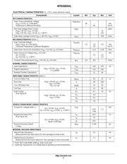
MAXIMUM RATINGS (T
C
= 25°C unless otherwise noted)
Rating
Symbol Value Unit
Drain–Source Voltage V
DSS
60 Vdc
Drain–Gate Voltage (R
GS
= 1.0 MΩ) V
DGR
60 Vdc
Gate–Source Voltage
– Continuous
– Single Pulse (t
p
≤ 50 ms)
V
GS
V
GSM
±15
± 20
Vdc
Vpk
Drain Current – Continuous @ 25°C
Drain Current – Continuous @ 100°C
Drain Current – Single Pulse (t
p
≤ 10 µs)
I
D
I
D
I
DM
12
8.0
42
Adc
Apk
Total Power Dissipation @ 25°C
Derate above 25°C
Total Power Dissipation @ T
A
= 25°C, when
mounted to minimum recommended pad
size
P
D
48
0.32
1.75
Watts
W/°C
Watts
Operating and Storage Temperature
Range
T
J
, T
stg
–55 to
175
°C
Single Pulse Drain–to–Source Avalanche
Energy – Starting T
J
= 25°C
(V
DD
= 25 Vdc, V
GS
= 5.0 Vdc,
I
L
= 12 Apk, L = 1.0 mH, R
G
= 25 Ω)
E
AS
72 mJ
Thermal Resistance
– Junction to Case
– Junction to Ambient
– Junction to Ambient, when mounted to
minimum recommended pad size
R
θJC
R
θJA
R
θJA
3.13
100
71.4
°C/W
Maximum Temperature for Soldering
Purposes, 1/8″ from case for 10
seconds
T
L
260 °C
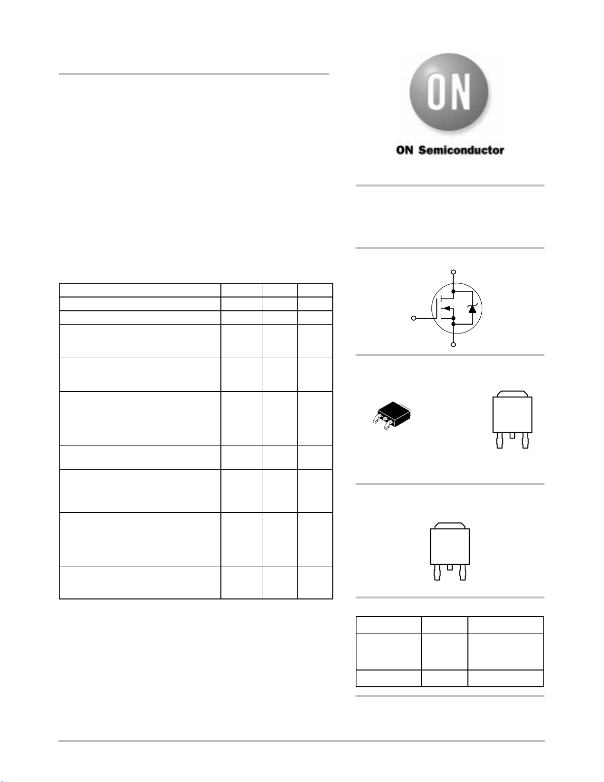
PIN ASSIGNMENT
1
Gate
3
Source
2
Drain
4
Drain
12 AMPERES
60 VOLTS
R
DS(on)
= 180 mΩ
Device Package Shipping
ORDERING INFORMATION
MTD3055VL DPAK 75 Units/Rail
CASE 369A
DPAK
STYLE 2
http://onsemi.com
N–Channel
D
S
G
MTD3055VL1 DPAK 75 Units/Rail
Preferred devices are recommended choices for future use
and best overall value.
MARKING
DIAGRAM
Y = Year
WW = Work Week
T = MOSFET
YWW
T
3055VL
MTD3055VLT4 DPAK 2500 Tape & Reel
1
2
3
4
Verzeichnis