
herunterladen
AN1987
1
RF Application Information
Freescale Semiconductor
Quiescent Current Control for the RF
Integrated Circuit Device Family
By: James Seto
INTRODUCTION
This application note introduces a bias control circuit that
can be used with the Freescale family of RF integrated
circuits. The MHVIC915 device is used as an example in this
paper, but the principle and theory of this controller can also
be applied to other IC devices such as the MW4IC915,
MWIC930, MW4IC2020, MW4IC2230 and MW5IC2030.
The quiescent current management of LDMOS devices
has a strong effect on its performance because the critical RF
performance parameters, such as intermodulation distortion
products, are dependent on the quiescent current level [1].
The control goal of the bias circuitry is to maintain the
quiescent current constant in all amplifier stages even if the
environmental and device temperature changes
significantly. Carefully selecting the control strategy will
optimize the device’s linearity performance and enable the
built-in quiescent current thermal tracking circuit to work
properly.
This application note examines the built-in quiescent
current thermal tracking system characteristics of the
MHVIC915 device and introduces several bias control
strategies. Verifications of the typical circuit performance are
also provided.
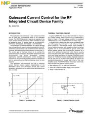
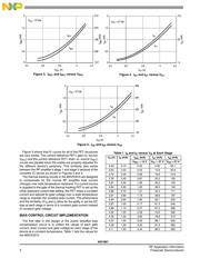
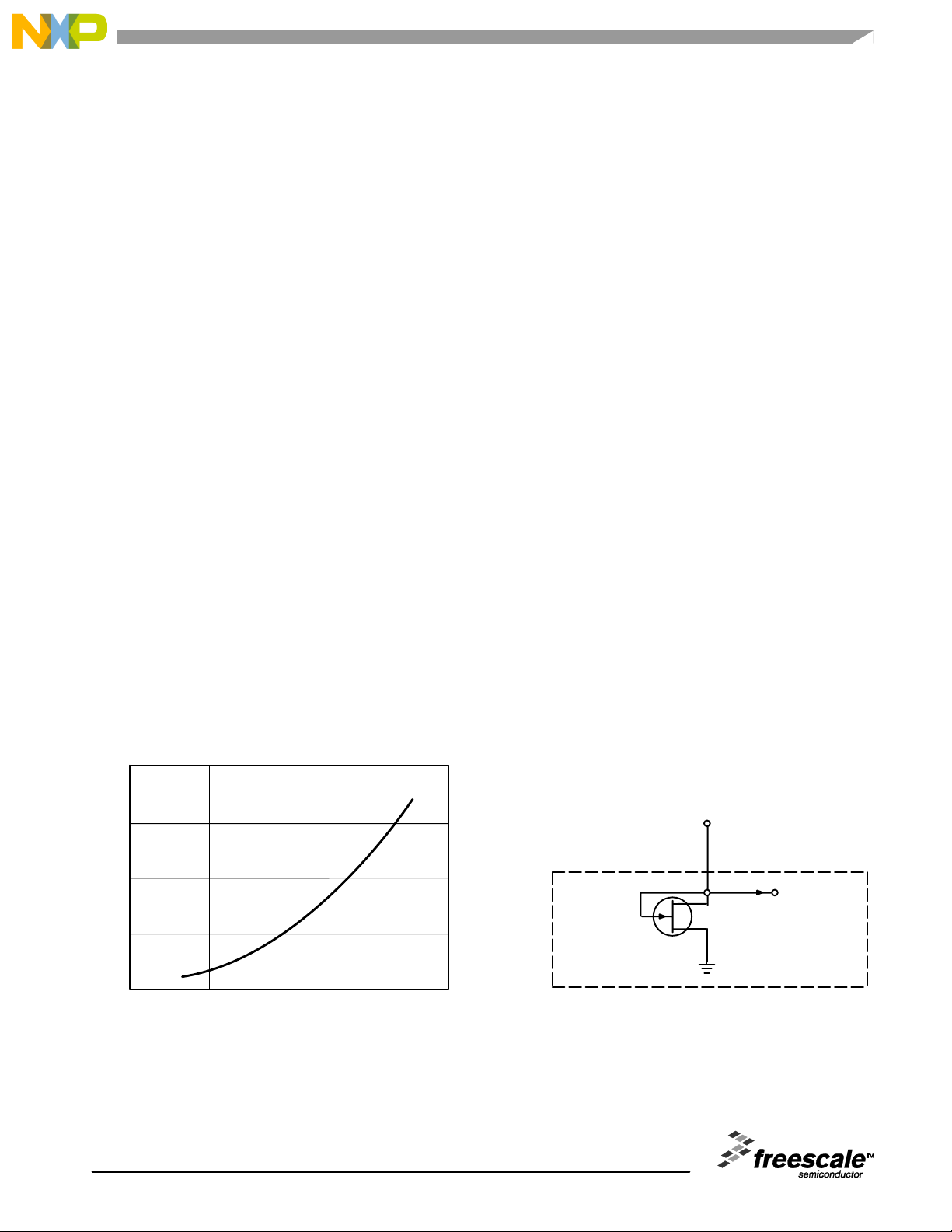
THERMAL TRACKING CIRCUIT
A typical LDMOS FET IV curve (Current, Drain-to - Source
(I
DS
) versus Voltage, Gate-to - Source (V
GS
)) relationship is
shown in Figure 1. The gate leakage current of the traditional
LDMOS device is very small (less than one micro amp).
In the MHVIC915 device, the gate current is relatively large
due to the supply requirements of the built - in thermal tracking
circuit (Figure 2). The thermal tracking circuit contains a
thermal tracking transistor with its gate and drain connected
together and its source connected to ground, along with
several voltage settings and current limiting resistors. As a
result of the additional components in this thermal tracking
circuit, the gate current draw is in the milliamp range (not in the
micro amp range) and follows the change of the drain current
(Figure 3). The thermal tracking circuit is physically located on
the die right next to the active RF LDMOS die area so its
operating temperature is closely tied to that of the main
amplifier circuit. The MHVIC915 has three major subcircuits,
each with their own thermal tracking circuit:
• Bias reference FET for self-bias application
• Active RF LDMOS amplifier stage 1 driver section
• Stage 2 output section [2].
V
GS
V
GS
Figure 1. I
DS
versus V
GS
Figure 2. Thermal Tracking Circuit
4.2
0
4
3.4
V
GS
(V)
V
DS
= 12 Vdc
3
2
1
3.6 3.8 4
I
DS
(mA)
AN1987
Rev. 1, 5/2004
Freescale Semiconductor
Application Note
Freescale Semiconductor, Inc., 2004, 2009. All rights reserved.