


herunterladen

1 Introduction
This application note describes the migration from A13
topology of wireless charging transmitter reference design
made by Freescale to the B5 topology of wireless charging
transmitter. Both transmitter topologies are suitable for the
automotive market. In the B5 transmitter design in comparison
to the A13 transmitter design, lower BOM (Bill of Material)
can be achieved, but on the other hand the A13 design has
better EMC radiation results.
2
A13/B5 comparison
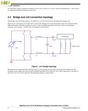
2.1 Coils
A13 design has three litz wire coils, each coil can be
connected independently, there is no possibility to charge with
two coils connected simultaneously. B5 design has four PCB
coils. This transmitter topology allows to connect two coils
simultaneously to achieve better charging performance and
active area efficiency for the case when the receiver is placed
between two coils. This possibility requires additional switch
Freescale Semiconductor
Document Number: AN5059
Application Note
Rev 0, 01/2015
Migration from A13 to B5 Wireless
Charging Transmitter
by: Vaclav Halbich
© 2015 Freescale Semiconductor, Inc.
Contents
1 Introduction................................................................1
2 A13/B5 comparison............................. ..................... 1
2.1 Coils................................................................1
2.2 Bridge and coil connection
topology........................................ .................2
2.3 Control of transferred energy.........................3
3 HW required changes................................................ 3
3.1 Multiplexer.....................................................3
3.2 Tuning capacitor.............................................3
3.3 DC/DC converter..................... ...................... 3
3.4 Coils............................. .................................. 4
4 HW PWM drivers.......................... ...........................4
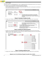
5 SW required changes...................... .......................... 4
5.1 Number of coils..............................................4
5.2 Ports adjustment.................... .........................5
5.3 Multiplexer.....................................................5
5.4 Peripherals modification................................ 5
5.5 Control of power transfer............................... 5
5.6 SW PWM drivers........................................... 5
5.7 NVM parameters................... .........................5
6 Conclusion.................................................................7