

herunterladen
© Semiconductor Components Industries, LLC, 2005
December, 2005 − Rev. 0
1 Publication Order Number:
NB4N11S/D
NB4N11S
3.3 V 1:2 AnyLevel™ Input
to LVDS Fanout Buffer /
Translator
The NB4N11S is a differential 1:2 Clock or Data Receiver and will
accept AnyLevel
TM
input signals: LVPECL, CML, LVCMOS,
LVTTL, or LVDS. These signals will be translated to LVDS and two
identical copies of Clock or Data will be distributed, operating up to
2.0 GHz or 2.5 Gb/s, respectively. As such, the NB4N11S is ideal for
SONET, GigE, Fiber Channel, Backplane and other Clock or Data
distribution applications.
The NB4N11S has a wide input common mode range from
GND + 50 mV to V
CC
− 50 mV. Combined with the 50 W internal
termination resistors at the inputs, the NB4N11S is ideal for
translating a variety of differential or single−ended Clock or Data
signals to 350 mV typical LVDS output levels.
The NB4N11S is functionally equivalent to the EP11, LVEP11,
SG11 or 7L11M devices and is offered in a small 3 mm X 3 mm
16−QFN package. Application notes, models, and support
documentation are available at www.onsemi.com.
Features
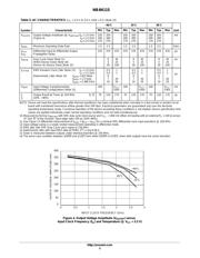
• Maximum Input Clock Frequency > 2.0 GHz
• Maximum Input Data Rate > 2.5 Gb/s
• 1 ps Maximum of RMS Clock Jitter
• Typically 10 ps of Data Dependent Jitter
• 380 ps Typical Propagation Delay
• 120 ps Typical Rise and Fall Times
• Functionally Compatible with Existing 3.3 V LVEL, LVEP, EP, and
SG Devices
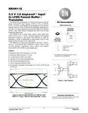
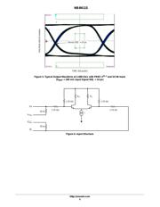
TIME (58 ps/div)
Figure 2. Typical Output Waveform at 2.488 Gb/s with
PRBS 2
23−1
(V
INPP
= 400 mV; Input Signal DDJ = 14 ps)
VOLTAGE (130 mV/div)
Device DDJ = 10 ps
A = Assembly Location
L = Wafer Lot
Y = Year
W = Work Week
*For additional marking information, refer to
Application Note AND8002/D.
MARKING
DIAGRAM*
QFN−16
MN SUFFIX
CASE 485G
http://onsemi.com
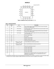
See detailed ordering and shipping information in the package
dimensions section on page 9 of this data sheet.
ORDERING INFORMATION
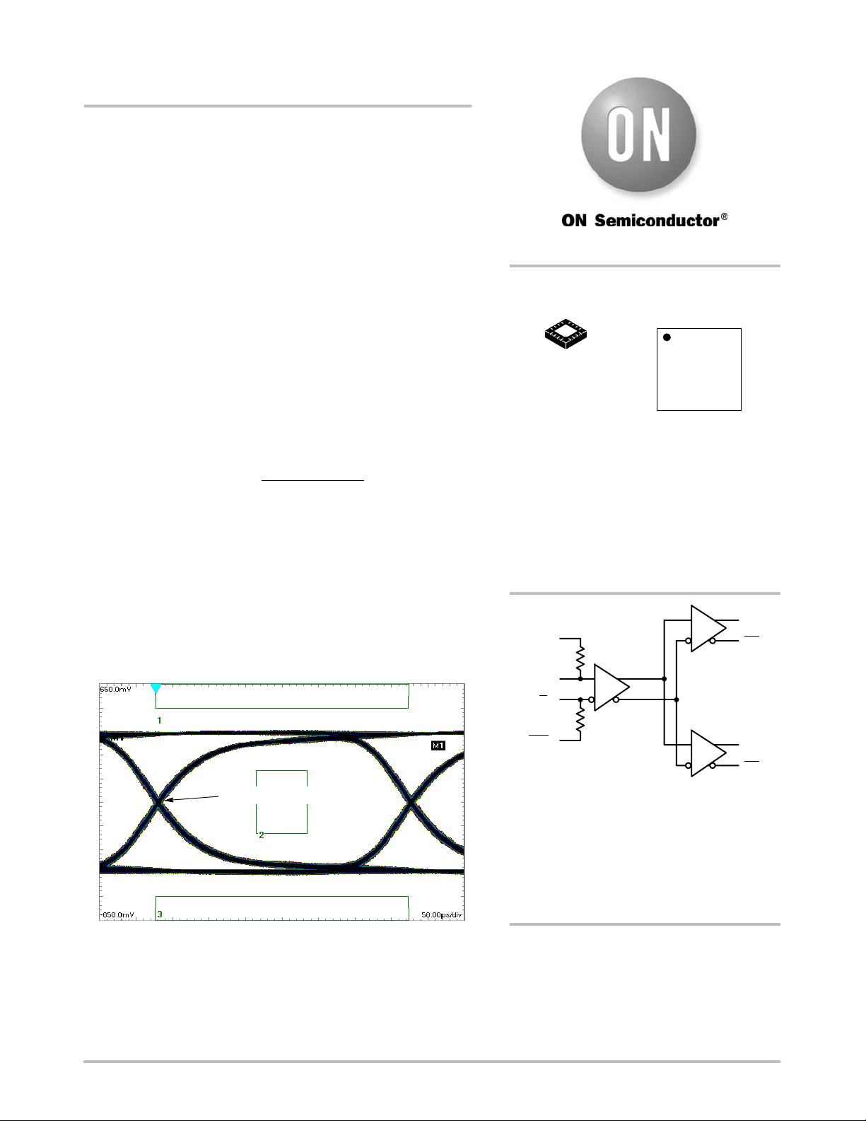
16
NB4N
11S
ALYW
1
1
Q0
Q0
Q1
Q1
D
D
V
TD
V
TD
Figure 1. Logic Diagram
Verzeichnis
- ・ Konfiguration des Pinbelegungsdiagramms on Seite 2
- ・ Abmessungen des Paketumrisses on Seite 10
- ・ Paket-Footprint-Pad-Layout on Seite 10
- ・ Teilenummerierungssystem on Seite 1 Seite 9 Seite 10
- ・ Markierungsinformationen on Seite 1
- ・ Typisches Anwendungsschaltbild on Seite 1
- ・ Technische Daten on Seite 9