
herunterladen
© Semiconductor Components Industries, LLC, 2016
August, 2016 − Rev. 6
1 Publication Order Number:
NB7L216/D
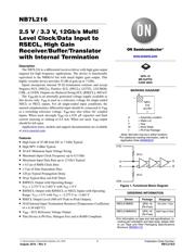
NB7L216
2.5 V / 3.3 V, 12Gb/s Multi
Level Clock/Data Input to
RSECL, High Gain
Receiver/Buffer/Translator
with Internal Termination
Description
The NB7L216 is a differential receiver/driver with high gain output
targeted for high frequency applications. The device is functionally
equivalent to the NBSG16 but with much higher gain output. This
highly versatile device provides 35 dB of gain up to 7 GHz.
Inputs incorporate internal 50 W termination resistors and accept
Negative ECL (NECL), Positive ECL (PECL), LVTTL, LVCMOS,
CML, or LVDS. Outputs are Reduced Swing ECL (RSECL), 400 mV.
The V
BB
pin is an internally generated voltage supply available to
this device only. V
BB
is used as a reference voltage for single-ended
NECL or PECL inputs. For all single-ended input conditions, the
unused complementary differential input should be connected to V
BB
as a switching reference voltage. V
BB
may also rebias AC coupled
inputs. When used, decouple V
BB
via a 0.01 mF capacitor and limit
current sourcing or sinking to 0.5 mA. When not used, V
BB
output
should be left open.
Application notes, models and support documentation are available
at www.onsemi.com
.
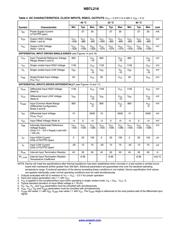
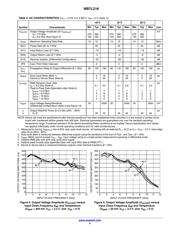
Features
• High Gain of 35 dB from DC to 7 GHz Typical
• High IIP3: 0 dBm Typical
• 20 mV Minimum Input Voltage Swing
• Maximum Input Clock Frequency up to 8.5 GHz
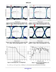
• Maximum Input Data Rate up to 12 Gb/s Typical
• < 0.5 ps of RMS Clock Jitter
• < 9 ps of Data Dependent Jitter
• 120 ps Typical Propagation Delay
• 30 ps Typical Rise and Fall Times
• RSPECL Output with Operating Range:
V
CC
= 2.375 V to 3.465 V with V
EE
= 0 V
• RSNECL Output with RSNECL or NECL Inputs with Operating
Range: V
CC
= 0 V with V
EE
= −2.375 V to −3.465 V
• RSECL Output Level (400 mV Peak-to-Peak Output),
• 50 W Internal Input Termination Resistors (Temperature-Coefficient
of < 6.38 mW/°C)
• V
BB
– ECL Reference Voltage Output
• This Device is Pb-Free, Halogen Free and is RoHS Compliant
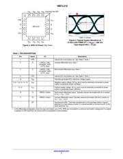
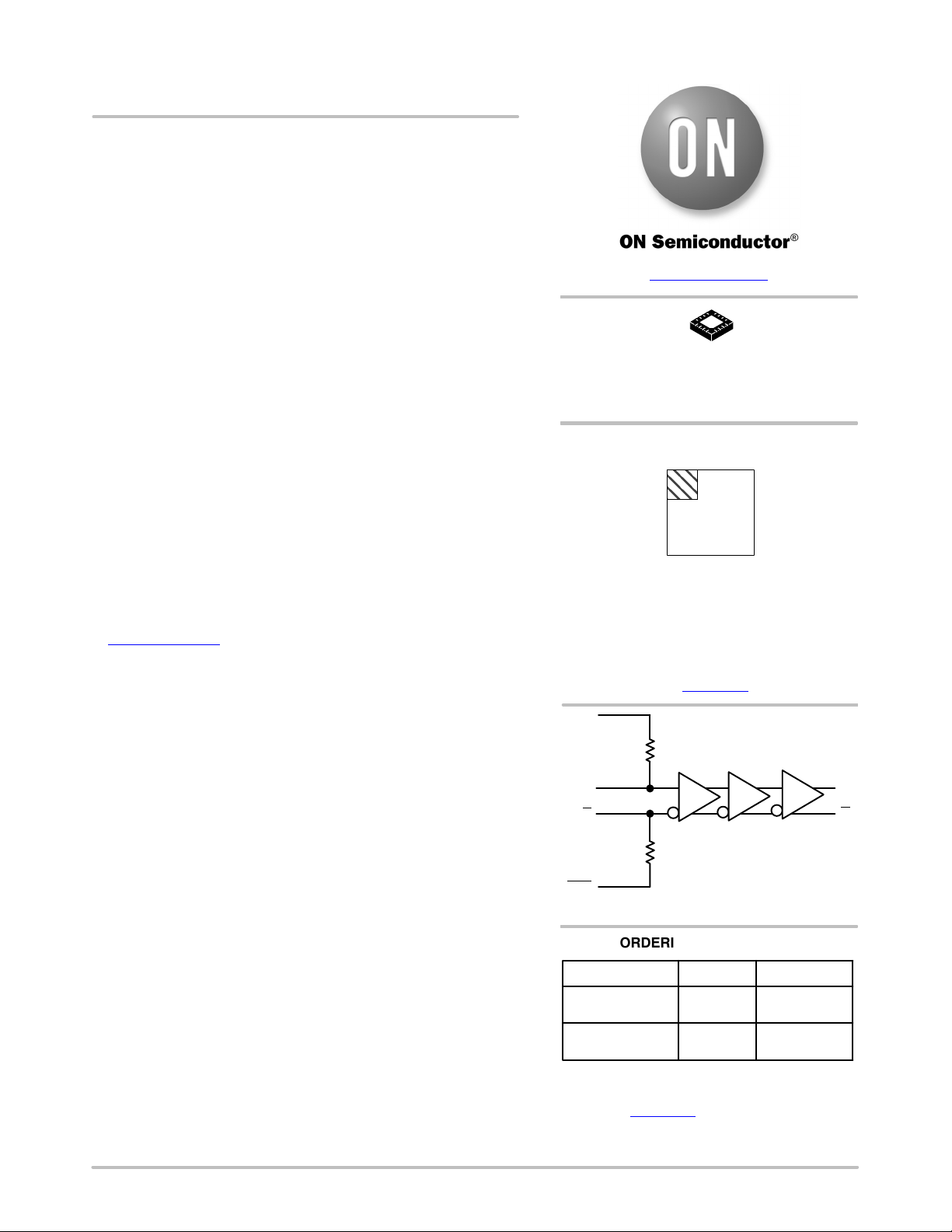
50 W
50 W
VTD
D
D
VTD
Q
Q
QFN−16
MN SUFFIX
CASE 485G
MARKING DIAGRAM*
*For additional marking information, refer to
Application Note AND8002/D
.
A = Assembly Location
L = Wafer Lot
Y = Year
W = Work Week
G = Pb-Free Package
Figure 1. Functional Block Diagram
www.onsemi.com
(Note: Microdot may be in either location)
1
16
NB7L
216
ALYWG
G
1
ÇÇÇ
ÇÇÇ
ORDERING INFORMATION
Device Package Shipping†
NB7L216MNG
QFN−16
(Pb-Free)
123 Units / Tube
NB7L216MNR2G 3000 Tape & Reel
†For information on tape and reel specifications, in-
cluding part orientation and tape sizes, please refer
to our Tape and Reel Packaging Specifications
Brochure, BRD8011/D
.
QFN−16
(Pb-Free)
Verzeichnis
- ・ Konfiguration des Pinbelegungsdiagramms on Seite 2
- ・ Abmessungen des Paketumrisses on Seite 11
- ・ Paket-Footprint-Pad-Layout on Seite 11
- ・ Teilenummerierungssystem on Seite 1 Seite 11
- ・ Markierungsinformationen on Seite 1 Seite 11
- ・ Blockdiagramm on Seite 1
- ・ Technische Daten on Seite 1
- ・ Teilenummernliste on Seite 3