
herunterladen
© Semiconductor Components Industries, LLC, 2013
December, 2013 − Rev. 0
1 Publication Order Number:
NCP1032/D
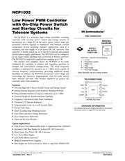
NCP1032
Low Power PWM Controller
with On-Chip Power Switch
and Startup Circuits for
Telecom Systems
The NCP1032 is a miniature high−voltage monolithic switching
converter with on−chip power switch and startup circuits. It
incorporates in a single IC all the active power control logic and
protection circuitry required to implement, with minimal external
components several switching regulator applications, such as a
secondary side bias supply or a low power DC−DC converter. This
converter is ideally suited for 24 V and 48 V telecom and medical
isolated power supply applications. The NCP1032 can be configured
in any single−ended topology such as forward or flyback converter.
The NCP1032 is targeted for applications requiring up to 3 W.
The internal error amplifier allows the NCP1032 to be easily
configured for secondary or primary side regulation operation in
isolated and non−isolated configurations. The fixed frequency
oscillator is optimized for operation up to 1 MHz and is capable of
external frequency synchronization, providing additional design
flexibility. In addition, the NCP1032 incorporates undervoltage and
overvoltage line detectors, programmable cycle−by−cycle current
limit, internal soft−start, and thermal shutdown to protect the
controller under fault conditions.
Features
• On Chip High 200 V Power Switch Circuit and Startup Circuit
• Internal Startup Regulator with Auxiliary Winding Override
• Programmable Oscillator Frequency Operation up to 1 MHz
• External Frequency Synchronization Capability
• Frequency Fold−down Under Fault Conditions
• Trimmed ± 1% Internal Reference
• Programmable Cycle−by−Cycle Current Limit
• Internal Soft−Start
• Active Leading Edge Blanking Circuit
• Line Under and Over Voltage Protection
• Over Temperature Protection
• These are Pb−Free Devices
Typical Applications
• POE (Power Over Ethernet)/PD. Refer to Application Note AND8247
• Secondary Side Bias Supply for Isolated DC−DC Converters
• Stand Alone Low Power DC−DC Converter
• Low Power Bias Supply
• Low Power Boost Converter
• Medical Isolated Power Supplies
• Bias Supply for Telecom Systems. Refer to App Note AND8119/D
http://onsemi.com
MARKING
DIAGRAMS
NCP1032 = Specific Device Marking
x = A or B
A = Assembly Location
L = Wafer Lot
Y = Year
W = Work Week
G = Pb−Free Package
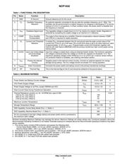
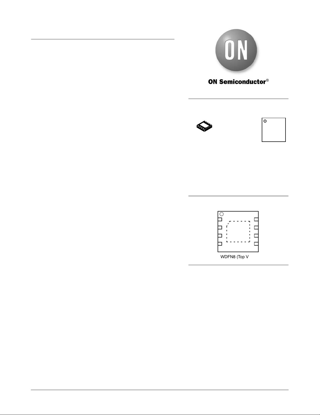
PIN CONNECTIONS
(Note: Microdot may be in either location)
See detailed ordering and shipping information in the package
dimensions section on page 20 of this data sheet.
ORDERING INFORMATION
WDFN−8
MN SUFFIX
CASE 511BH
1032x
ALYW G
G
ÇÇ
ÇÇ
ÇÇ
ÇÇ
Ç
Ç
Ç
Ç
WDFN8 (Top View)
GND
GND
C
T
V
FB
COMP
V
CC
V
DRAIN
CL
UV/OV
1
Verzeichnis
- ・ Konfiguration des Pinbelegungsdiagramms on Seite 1 Seite 3
- ・ Abmessungen des Paketumrisses on Seite 21
- ・ Paket-Footprint-Pad-Layout on Seite 18 Seite 21
- ・ Teilenummerierungssystem on Seite 1 Seite 20 Seite 21
- ・ Markierungsinformationen on Seite 1 Seite 20 Seite 21
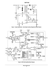
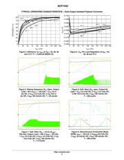
- ・ Blockdiagramm on Seite 2 Seite 17
- ・ Typisches Anwendungsschaltbild on Seite 1 Seite 2 Seite 17 Seite 20
- ・ Beschreibung der Funktionen on Seite 3
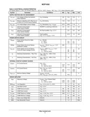
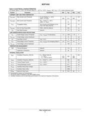
- ・ Technische Daten on Seite 20
- ・ Anwendungsbereich on Seite 1 Seite 17
- ・ Elektrische Spezifikation on Seite 4 Seite 5