
herunterladen

© Semiconductor Components Industries, LLC, 2008
September, 2008 − Rev. 1
1 Publication Order Number:
AND8318/D
AND8318/D
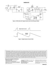
Offline Buck Converter with
Tapped Inductor Offers
Improved Performance
Prepared by: Frank Cathell
Introduction
For electronic and industrial equipment requiring
non−isolated, offline, low power outputs, the simple buck
converter appears ideal; however, the large differential
input−to−output voltage can be problematic in terms of very
low converter duty cycle, peak−to−average switching
current ratios, and overall conversion efficiency. This
application presents a solution that will overcome many of
these issues without additional electronic circuitry. The
solution involves a modification to the buck inductor in
which a tap is added to the winding and the buck
freewheeling diode is connected to the tap. This magnetic
reconfiguration will convert the standard buck topology
shown in Figure 1 to what is sometimes referred to as the
“current−boosted” buck shown in Figure 2.
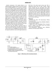
Buck Converter Operation
A conventional offline buck converter with an output of
12 volts at 300 mA (3.6 watts) is shown in Figure 1. This
example converter is configured around ON
Semiconductor’s NCP1014 monolithic current mode
controller with integrated MOSFET for maximum circuit
simplicity; however, it could also be configured with a
discrete controller such as the NCP1216 and a separate
MOSFET. Voltage regulation and feedback are
accomplished via the simple network of Zener diode Z1, the
associated resistors R2 and R3, and optocoupler U2. The
optocoupler is necessary because the ground (pin 4) on the
NCP1014 controller is at a switching node and optical
feedback is the simplest and most economical way to
overcome the associated dV/dts and high voltage issues
associated with other types of discrete feedback and/or
voltage offset circuits. The schematic also includes a simple
conducted EMI filter comprised of C1, and pi−network C2,
L1, and C3.
As with typical buck operation, the rectified offline
voltage at bulk capacitor C3 provides a dc level to the drain
of U1’s internal MOSFET (pin 3), and is switched on and off
at the source terminal (pin 4) and presented to the integrating
circuit of L2 and C4. The L/C output filter averages the
switched rectangular waveform to the desired output dc
voltage at C4 via the voltage sensing/feedback of Z1/U2 and
pulse width modulation in U1. Freewheeling diode D5
provides for current continuity in L2 when the MOSFET in
U1 is in the offstate.
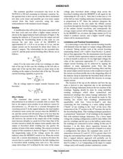
The dc transfer function of the buck converter is given by
Vout = D x Vin where D is the duty cycle (MOSFET on time
divided by total switching period T) of the rectangular wave
presented at L2’s input. Vin is the dc voltage presented to the
buck switching circuit. For a nominal input of 120 Vac and
an output of 12 volts one can easily calculate the required
duty cycle D for the internal MOSFET switch:
D +
V
out
(V
in
ac 1.4)
+
12
(120 1.4)
+ 0.07 or 7%
This is a very small duty cycle, which for a switching
frequency of 100 kHz (T = 10 ms), amounts to an on time of
0.07 x 10 ms = 0.7 ms or 700 ns. This short on time duration
is actually not much larger than the controller’s internal
propagation delay and leaves little room for pulse width
dynamic range for load changes, and will certainly result in
a sub−switching frequency pulse skipping mode of
operation when the load drops below the level where L2’s
current becomes discontinuous. Operation in this mode may
be acceptable as long as the output ripple of the supply is not
excessive and/or audible noise is not present in the inductor.
Operation with low duty cycles also requires the
inductance of the main output choke L2 to be higher if
discontinuous conduction mode (DCM) is to be avoided at
the lowest nominal output loading. This aspect of the
inductor design is also related to the peak−to−average
current ratio seen by the MOSFET. The peak current through
the internal MOSFET of U1 is the sum of the output load
current and the magnetizing current of L2. Under nominal
line conditions (165 Vdc on C3), the peak magnetizing
current at the end of a switching cycle is given by the familiar
relationship of E = L x dI/dt. Rearranging the terms for dI
gives dI = (E x dt)/L, which computes to the following
magnetizing current for this example:
dI +
[(V
in
dc*V
out
) dt]
L
+
[(165*12) 0.7]
750 mH
+ 143 mA
Peak MOSFET current will be 300 mA (max load current)
+ 143 mA = 443 mA.
APPLICATION NOTE
http://onsemi.com