


herunterladen
© Semiconductor Components Industries, LLC, 2009
February, 2009 − Rev. 16
1 Publication Order Number:
NCP551/D
NCP551, NCV551
150 mA CMOS Low Iq
Low-Dropout Voltage
Regulator
The NCP551 series of fixed output low dropout linear regulators are
designed for handheld communication equipment and portable battery
powered applications which require low quiescent. The NCP551
series features an ultra−low quiescent current of 4.0 mA. Each device
contains a voltage reference unit, an error amplifier, a PMOS power
transistor, resistors for setting output voltage, current limit, and
temperature limit protection circuits.
The NCP551 has been designed to be used with low cost ceramic
capacitors and requires a minimum output capacitor of 0.1 mF. The
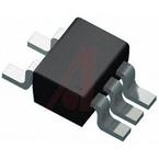
device is housed in the TSOP−5 surface mount package. Standard
voltage versions are 1.4, 1.5, 1.8, 2.5, 2.7, 2.8, 2.9, 3.0, 3.1, 3.2, 3.3,
and 5.0 V. Other voltages are available in 100 mV steps.
Features
• Low Quiescent Current of 4.0 mA Typical
• Maximum Operating Voltage of 12 V
• Low Output Voltage Option
• High Accuracy Output Voltage of 2.0%
• Industrial Temperature Range of −40°C to 85°C
(NCV551, T
A
= −40°C to +125°C)
• NCV Prefix for Automotive and Other Applications Requiring Site
and Control Changes
• Pb−Free Packages are Available
Typical Applications
• Battery Powered Instruments
• Hand−Held Instruments
• Camcorders and Cameras
Figure 1. Representative Block Diagram
Driver w/
Current
Limit
V
in
V
out
Thermal
Shutdown
Enable
GND
OFF
ON
1
3
5
2
See detailed ordering and shipping information in the package
dimensions section on page 9 of this data sheet.
ORDERING INFORMATION
TSOP−5
(SOT23−5, SC59−5)
SN SUFFIX
CASE 483
PIN CONNECTIONS AND
MARKING DIAGRAM
1
3
N/C
V
in
2GND
Enable
4
V
out
5
(Top View)
http://onsemi.com
xxxAYWG
G
xxx = Specific Device Code
A = Assembly Location
Y = Year
W = Work Week
G = Pb−Free Package
(Note: Microdot may be in either location)
1
5
Verzeichnis
- ・ Konfiguration des Pinbelegungsdiagramms on Seite 1
- ・ Abmessungen des Paketumrisses on Seite 11
- ・ Paket-Footprint-Pad-Layout on Seite 11
- ・ Teilenummerierungssystem on Seite 1 Seite 9 Seite 10 Seite 11
- ・ Markierungsinformationen on Seite 1 Seite 9 Seite 10
- ・ Blockdiagramm on Seite 1
- ・ Typisches Anwendungsschaltbild on Seite 1 Seite 8
- ・ Beschreibung der Funktionen on Seite 2
- ・ Anwendungsbereich on Seite 1 Seite 8
- ・ Elektrische Spezifikation on Seite 3