


herunterladen
© Semiconductor Components Industries, LLC, 2009
May, 2009 − Rev. 3
1 Publication Order Number:
NCP1532/D
NCP1532
Dual Output Step-Down
Converter 2.25 MHz
High-Efficiency, Out of
Phase Operation, Low
Quiescent Current, Source
up to 1.6 A
The NCP1532 dual step down DCDC converter is a monolithic
integrated circuit dedicated to supply core and I/O voltages of new
multimedia design in portable applications powered from 1−cell
Li−ion or 3 cell Alkaline / NiCd / NiMH batteries.
Both channels are externally adjustable from 0.9 V to 3.3 V and can
source totally up to 1.6 A, 1.0 A maximum per channel. Converters are
running at 2.25 MHz switching frequency which reduces component
size by allowing the use of small inductor (down to 1 mH) and
capacitors and operates 180° out of phase to reduce large amount of
current demand on the battery. Automatic switching PWM/PFM mode
and synchronous rectification offer improved system efficiency. The
device can also operate into fixed frequency PWM mode for low noise
applications where low ripple and good load transients are required.
Additional features include integrated soft−start, cycle−by−cycle
current limit and thermal shutdown protection. The device can also be
synchronized to an external clock signal in the range of 2.25 MHz.
The NCP1532 is available in a space saving, ultra low profile
3x3 x 0.55 mm 10 pin mDFN package.
Features
• Up to 97% Efficiency
• 50 mA Quiescent Current
• Synchronous Rectification for Higher Efficiency
• 2.25 MHz Switching Frequency, 180° Out of Phase
• Sources up to 1.6 A, 1.0 A Maximum per Channel
• Adjustable Output Voltage from 0.9 V to 3.3 V
• Mode Selection Pin: Eco Mode or Low Noise Mode
• 2.7 V to 5.5 V Input Voltage Range
• Thermal Limit Protection
• Short Circuit Protection
• All pins are fully ESD Protected
• This is a Pb−Free Device
Typical Applications
• Cellular Phones, Smart Phones and PDAs
• Digital Still Cameras
• MP3 Players and Portable Audio Systems
• Wireless and DSL Modems
• Portable Equipment
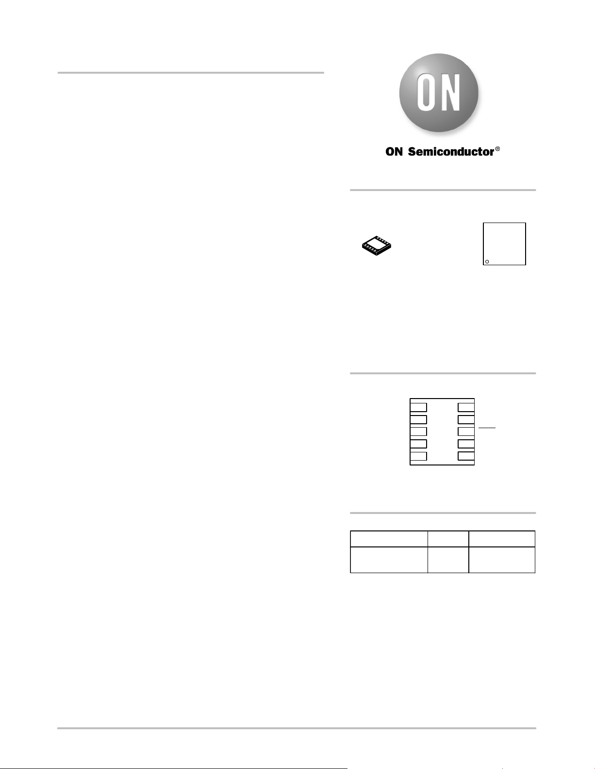
PIN CONNECTION
MARKING
DIAGRAM
http://onsemi.com
UDFN10
MU SUFFIX
CASE 506AT
1532
AA
AaLYWG
G
FB1
FB2
EN1
VIN
SW1
EN2
SW2
110
2
3
4
9
8
7
GND
5
MODE/
SYNC
6
POR
(Top View)
UDFN10
Aa = Assembly Location
(may be 1 or 2 characters)
L = Wafer Lot
Y = Year
W = Work Week
G = Pb−Free Package
(Note: Microdot may be in either location)
Device Package Shipping
†
ORDERING INFORMATION
NCP1532MUAATXG UDFN10
(Pb−Free)
3000 /
Tape & Reel
†For information on tape and reel specifications,
including part orientation and tape sizes, please
refer to our Tape and Reel Packaging Specifications
Brochure, BRD8011/D.
Verzeichnis
- ・ Konfiguration des Pinbelegungsdiagramms on Seite 1
- ・ Abmessungen des Paketumrisses on Seite 16
- ・ Paket-Footprint-Pad-Layout on Seite 16
- ・ Teilenummerierungssystem on Seite 1 Seite 16
- ・ Markierungsinformationen on Seite 1
- ・ Blockdiagramm on Seite 3
- ・ Typisches Anwendungsschaltbild on Seite 1 Seite 2
- ・ Beschreibung der Funktionen on Seite 2
- ・ Technische Daten on Seite 1
- ・ Anwendungsbereich on Seite 1
- ・ Elektrische Spezifikation on Seite 5 Seite 6